Fundamentals of Sigma-Delta ADCs Jinseok Koh, Ph.D. Texas - PowerPoint PPT Presentation
Fundamentals of Sigma-Delta ADCs Jinseok Koh, Ph.D. Texas Instruments Inc. Dallas, TX IEEE SSCS Dallas Chapter, June 2007 Jinseok Koh (jinseok@ti.com) Why Analog to Digital Conversion? Naturally occurring signals are analog signal
Fundamentals of Sigma-Delta ADCs Jinseok Koh, Ph.D. Texas Instruments Inc. Dallas, TX IEEE SSCS Dallas Chapter, June 2007 Jinseok Koh (jinseok@ti.com)
Why Analog to Digital Conversion? � Naturally occurring signals are analog signal � Human beings perceive and retain information in analog form � BUT, Analog signal is more sensitive to noise than digital signal Jinseok Koh (jinseok@ti.com)
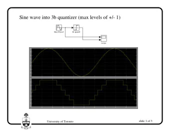
How Analog to Digital Conversion? 110 101 101 101 101 101 100 100 100 011 010 010 010 010 001 000 t 1 t 2 t 3 t 4 t 5 t 6 t 7 t 8 t 9 1. Sample analog signal 2. Quantize sampled analog signal � Quantization noise 3. Faster sampling time, better accuracy 4. Higher quantization levels, better accuracy Jinseok Koh (jinseok@ti.com)
Continuous Time Signal Amplitude Time f B , band of Signal interest Power 0 f C f B Frequency Signal frequency, f C = band of interest, f B (Maximum frequency of the signal) Jinseok Koh (jinseok@ti.com)
Jinseok Koh (jinseok@ti.com)
Typical Architecture for Analog to Digital Conversion ADC Continuous Sampled Digital Analog Time Signal Analog Signal Signal Signal Anti Aliasing Quantization DSP S/H Filter Jinseok Koh (jinseok@ti.com)
Nyquist Rate vs. Oversampled Jinseok Koh (jinseok@ti.com)
Modeling of Quantizer • Quantizer is non-linear building block – Need modeling for simplifying the analysis • White additive noise assumptions – It is not fulfilled in many applications, However – It makes analysis easy and makes possible the use of z-tansformation Jinseok Koh (jinseok@ti.com)
Quantization Noise • Quantity of in-band noise depends on the over-sampling ratio 2 ) -10log(s n 2 ) +3.01r(dB), where – SNR = 10log(s x 2 and s n 2 are input signal power and in-band noise power respectively, and – s x r is defined by over-sampling ratio, f s /2f b =2 r – Pervez M. Aziz, “An overview of sigma-delta converters,” IEEE Signal processing Magazine, pp 61-84, Jan. 1996 Jinseok Koh (jinseok@ti.com)
Over-sampling and Noise Shaping Every doubling of sampling frequency 1RL V H leads approximately 3 dB enhancement in SNR % D Q G � RI�,Q W H U H V W I V I V I V Noise shaping pushes quantization noise to higher frequency resulting in suppressing Q. noise in the band of interest Jinseok Koh (jinseok@ti.com)
How to Shape the noise? H(z) 1 = ⋅ + ⋅ Y(z) X(z) E(z) + + 1 H(z)G(z) 1 H(z)G(z) STF NTF If H(z) = z -1 /1-z -1 and G(z)=1, NTF and STF will be: Y(z) Y(z) − − = = 1 = = − 1 STF Z NTF 1 Z X(z) E(z) Jinseok Koh (jinseok@ti.com)
Jinseok Koh (jinseok@ti.com)
Jinseok Koh (jinseok@ti.com)
Jinseok Koh (jinseok@ti.com)
Example, 2 nd order Sigma-Delta ADC Output of the 1st integrator Output of the 2nd integrator � The dynamic range at the output of the two integrators is limited � Input signal attenuation by 6 dB Jinseok Koh (jinseok@ti.com)
Noise Shaping 2 nd order 1 st order Band of interest In-band quantization noise is suppressed more with 2 nd order Jinseok Koh (jinseok@ti.com)
Single-bit or Multi-bit ?S Single Bit • Feedback DAC inherently linear. So no HD distortion. • Need a faster Amplifier • Lower SQNR for a given modulator order Multi Bit • Gives higher SQNR • Relaxed opamp specs due to smaller step size • DAC non-linearity is a performance limit Require dynamic element matching • Jinseok Koh (jinseok@ti.com)
Summary • Sigma-delta ADC provide trade-offs between: – Power consumption, – Over-sampling ratio ( OSR ) – System performance ( SNR ) • High OSR implies: – Lower number of quantization levels – Lower modulator order, but – More demanding settling requirements for the analog building blocks Jinseok Koh (jinseok@ti.com)
A Sigma-Delta ADC with a built-in Anti-aliasing filter for Bluetooth receiver in 130 nm digital process Jinseok Koh Wireless Analog Technology Center Texas Instruments Inc. Dallas, TX Published in CICC2004 Jinseok Koh (jinseok@ti.com)
Introduction • RF input signal is amplified by two stage Amplifier, LNA and TA. • TA output is down converted and filtered by Direct-Sampling Mixer (DSM). • IFA amplifies mixer output signal operating at 75 Mhz. • Sigma-Delta ADC converts 75 MHz IFA output to 37.5 MHz digital words. Jinseok Koh (jinseok@ti.com)
ADC Requirements • 60 dB Dynamic range at 1 Mhz signal bandwidth – 2 nd order sigma-delta ADC – 5 level quantizer – 37.5 MHz sampling frequency. • Gain Control – O dB and 14 dB gain option is required for system AGC function. • Low Power consumption • Low cost Jinseok Koh (jinseok@ti.com)
Noise budget Noise Budget Conditions: 1. Fs=37.5 MHz 600 2. BW=1 MHz 3. 5 level Flash 500 (unit = µ V) 400 Noise [uVrms] Noise_tot Quant. Amp. kT/C Ref 564 561 75 18.8 18 300 200 100 0 Noise Quant. Amp. kT/C Ref Noise Sources • Quantization noise is a dominant noise source. – Unit capacitance element is selected based on considering mismatch effect. – Noises from amplifier and reference buffer are not critical. – Power consumption of amplifier is minimized since noise from it is negligible compared to the high in-band quantization noise. Jinseok Koh (jinseok@ti.com)
Required building blocks Decimation FIR Filter Buffer by 2 3bit Input out Sigma-Delta 2 x1 ADC • Based on power consumption and noise analysis, following functions are required. – Decimation by Two: sampling frequency 37.5 MHz can provides enough Dynamic Range utilizing 5 level flash ADC. – Anti-alias filtering: Decimation by two function causes folding noise. – Buffering: buffer amplifier is required to avoid charge sharing between Switched capacitor FIR filter and sampling circuits in Sigma-Delta ADC. Jinseok Koh (jinseok@ti.com)
Proposed Architecture Vin Z -1 Z -1 2 a2 1 - Z -1 1 - Z -1 b1 b2 3 Bit OUT ILA Decoder • Decimation, anti-aliasing filtering is merged with sampling circuits. – Saved power consumption and silicon area since it avoids the buffer. • Second order Sigma-Delta ADC with 5 level flash. • ILA DEM is used to suppress mismatch energy from DAC in feedback loop. Jinseok Koh (jinseok@ti.com)
FIR Anti-aliasing Filter = + − + − + − ( ) ( ) 3 ( 1 ) 3 ( 2 ) ( 3 ) y n x n x n x n x n -80 dB at 36.5 MHz • 60dB attenuation is required to suppress folding noise by system simulations. • Third order FIR filter is chosen and provides 80 dB attenuation at folding frequency band edge. Jinseok Koh (jinseok@ti.com)
FIR Anti-aliasing Filter and Decimation P1 P2 P3 C p1 Input P1 I2 P2 C p2 I1 P3 C p3 I3 P1 C p1, 3C p1 I1 I3 I2 P1 I1 I3 P2 P2 P3 C M C p2, 3C p2 P1 P2 3C p1 P3 I3 3C p2 I3 P3 3C p3 I1 C p3, 3C p3 I3 I3 I1 P4 I3 I3 I1 P1 P2 P3 C p4, 3C p4 P4 P5 P6 P5 C p4 I2 C p5 I1 C p6 I3 P4 P5 P6 C p5, 3C p5 P6 Vrefp 5 level I1 P4 I2 I1 I3 P5 P6 DAC I3 Vrefm C p6, 3C p6 I1 3C p4 3C p5 3C p6 P4 I1 P5 I2 P6 I2 I2 I1 I1 P4 I2 P5 I2 P6 I3 • 6 phase clock signals are utilized to implement FIR filter. • On Pi phase, input is sampled at Cpi and 3Cpi capacitors, • On I3 phase, Cp3, 3Cp2, 3Cp1 and Cp6 is dumped into integrating capacitor. Jinseok Koh (jinseok@ti.com)
Gain control High Gain mode LG C M Csh HG N1 Input N2 Cs N2 N1 • Gain control function is implemented in FIR sampling block by adding the high gain mode switched capacitor circuits in parallel with each capacitor in SC FIR filter. • Gain is defined by the ratio between sampling capacitors and integrating capacitor (C M ). Jinseok Koh (jinseok@ti.com)
Comparator Ci VINP Cr REFP N2 OUTM COMP Ci VINM OUTP N2 Cr LATCH REFM N1 N2 • Switched capacitor comparator is used to build 5 level quantizer. • Capacitor ratio between C i and C r is chosen to have threshold voltage for each comparator. • Capacitor size is optimized to be minimum considering decision speed, resolution (mismatch) and offset. Jinseok Koh (jinseok@ti.com)
Two Tone Measurements f 1 = 1 MHz f 2 = 2.2 MHz Number of FFT : 65536 IM3 • -8 dBFS sine signals at 1 MHz (f1) and 2.2 MHz (f2) are applied. • -80 dBc IM3 shows at 200 kHz. Jinseok Koh (jinseok@ti.com)
Measured SNDR 60 dB SNDR at –4 dBFS input SNDR vs. Input 70 60 50 SNDR [dB] 40 High Gain 30 Low Gain 20 10 0 -70 -60 -50 -40 -30 -20 -10 0 Input Amplitude [dBFS] • Peak SNDR for high gain mode is smaller since harmonics come earlier than low gain mode due to amplifier speed. Jinseok Koh (jinseok@ti.com)
Performance summary Technology 130nm Digital CMOS Process Sampling Frequency 37.5 MHz Signal Bandwidth 1 MHz Peak SNDR1 60 dB Peak SNDR2 57 dB Dynamic Range 67 dB Overall Dynamic Range 77 dB Input Range 1.4 V pp (differential) Power Consumption 1.6 mW Voltage Supply 1.58 V 0.2 mm 2 Core Area • Sinusoidal signal at 360 kHz is used for performance measurements. • Peak SNDR1 : when 0 dB gain option is selected. • Peak SNDR2 : when 14 dB gain option is selected. Jinseok Koh (jinseok@ti.com)
Recommend
More recommend
Explore More Topics
Stay informed with curated content and fresh updates.
