INTRODUCTION TO DELTA-SIGMA ADCS Richard Schreier - PDF document
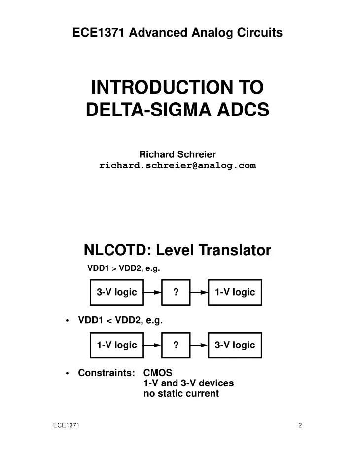
ECE1371 Advanced Analog Circuits INTRODUCTION TO DELTA-SIGMA ADCS Richard Schreier richard.schreier@analog.com NLCOTD: Level Translator VDD1 > VDD2, e.g. 3-V logic ? 1-V logic VDD1 < VDD2, e.g. 1-V logic ? 3-V logic
ECE1371 Advanced Analog Circuits INTRODUCTION TO DELTA-SIGMA ADCS Richard Schreier richard.schreier@analog.com NLCOTD: Level Translator VDD1 > VDD2, e.g. 3-V logic ? 1-V logic • VDD1 < VDD2, e.g. 1-V logic ? 3-V logic • Constraints: CMOS 1-V and 3-V devices no static current ECE1371 2
Highlights (i.e. What you will learn today) 1 1 st -order modulator (MOD1) Structure and theory of operation 2 Inherent linearity of binary modulators 3 Inherent anti-aliasing of continuous-time modulators 4 2 nd -order modulator (MOD2) 5 Good FFT practice ECE1371 3 0. Background (Stuff you already know) The SQNR * of an ideal n -bit ADC with a full-scale • sine-wave input is (6.02 n + 1.76) dB “6 dB = 1 bit.” • The PSD at the output of a linear system is the product of the input’s PSD and the squared magnitude of the system’s frequency response X YS yy f ) 2 S xx f H e j 2 π f ⋅ i.e. H ( z ) ( ) = ( ( ) • The power in any frequency band is the integral of the PSD over that band *. SQNR = Signal-to-Quantization-Noise Ratio ECE1371 4
1. What is ∆Σ ? ∆Σ is NOT a fraternity • Simplified ∆Σ ADC structure: • Analog Digital Loop Coarse Loop Coarse In Out Filter ADC Filter ADC (to digital filter) DAC DAC • Key features: coarse quantization, filtering, feedback and oversampling Quantization is often quite coarse (1 bit!), but the effective resolution can still be as high as 22 bits. ECE1371 5 What is Oversampling? • Oversampling is sampling faster than required by the Nyquist criterion For a lowpass signal containing energy in the ( , ) frequency range 0 f B , the minimum sample rate required for perfect reconstruction is f s 2 f B . = ≡ ⁄ ( ) • The oversampling ratio is OSR f s 2 f B ∼ • For a regular ADC, OSR 2 3 – To make the anti-alias filter (AAF) feasible For a ∆Σ ADC, ∼ • OSR 30 To get adequate quantization noise suppression. Signals between f B and ~ f s are removed digitally. ECE1371 6
Oversampling Simplifies AAF Desired Undesired OSR ~ 1: Signal Signals f ⁄ f s 2 First alias band is very close OSR = 3: Wide transition band f ⁄ Alias far away f s 2 ECE1371 7 How Does A ∆Σ ADC Work? Coarse quantization ⇒ lots of quantization error. • So how can a ∆Σ ADC achieve 22-bit resolution? A ∆Σ ADC spectrally separates the quantization • error from the signal through noise-shaping 1 t t –1 ∆Σ u v w Decimation analog digital ADC input Filter output n @2 f B 1 bit @ f s desired signal Nyquist-rate shaped undesired PCM Data noise signals ⁄ ⁄ f B f s 2 f B f s 2 f B ECE1371 8
A ∆Σ DAC System 1 t –1 ∆Σ u v w digital Reconstruction analog input Modulator Filter output 1 bit @ f s (interpolated) analog signal output shaped noise ⁄ ⁄ f B f s 2 f B f s 2 f B f s • Mathematically similar to an ADC system Except that now the modulator is digital and drives a low-resolution DAC, and that the out-of-band noise is handled by an analog reconstruction filter. ECE1371 9 Why Do It The ∆Σ Way? • ADC: Simplified Anti-Alias Filter Since the input is oversampled, only very high frequencies alias to the passband. A simple RC section often suffices. If a continuous-time loop filter is used, the anti-alias filter can often be eliminated altogether. • DAC: Simplified Reconstruction Filter The nearby images present in Nyquist-rate reconstruction can be removed digitally. + Inherent Linearity Simple structures can yield very high SNR. + Robust Implementation ∆Σ tolerates sizable component errors. ECE1371 10
2. MOD1: 1 st -Order ∆Σ Modulator [Ch. 2 of Schreier & Temes] Quantizer “ ∆ ” “ Σ ” v (1-bit) Y 1 y U V Q –1 z -1 Feedback DAC V’ v’ z -1 DAC v Since two points define a line, a binary DAC is inherently linear. ECE1371 11 MOD1 Analysis • Exact analysis is intractable for all but the simplest inputs, so treat the quantizer as an additive noise source: Y U V Q z -1 E z -1 Y V V(z) = Y(z) + E(z) Y(z) = ( U(z) – z -1 V(z) ) / (1–z -1 ) ⇒ (1–z -1 ) V(z) = U(z) – z -1 V(z) + (1–z -1 )E(z) V(z) = U(z) + (1–z –1 )E(z) ECE1371 12
The Noise Transfer Function (NTF) • In general, V(z) = STF(z)•U(z) + NTF(z)•E(z) For MOD1, NTF(z) = 1–z –1 • The quantization noise has spectral shape! Poles & zeros: NTF e j 2 π f 4 ) 2 ( 3 2 ≅ ω 2 ω for 1 « 1 0 0 0.1 0.2 0.3 0.4 0.5 Normalized Frequency ( f / f s ) • The total noise power increases, but the noise power at low frequencies is reduced ECE1371 13 In-band Quant. Noise Power σ e 2 • Assume that e is white with power 2 π S ee ω σ e ⁄ ( ) = i.e. • The in-band quantization noise power is ω B ω B σ e ∫ 2 ∫ H e j ω ) 2 S ee ω ( ) d ω ≅ ω 2 d ω IQNP - - - - - - = ( π 0 0 π 2 σ e π 2 ≡ ( ) 3 • Since OSR , IQNP - OSR – - - - - - - - = - - - - - - - - - - - - ω B 3 • For MOD1, an octave increase in OSR increases SQNR by 9 dB “1.5-bit/octave SQNR-OSR trade-off.” ECE1371 14
A Simulation of MOD1 0 Full-scale test tone –20 SQNR = 55 dB @ OSR = 128 dBFS/NBW –40 Shaped “Noise” –60 –80 20 dB/decade NBW = 5.7x10 –6 –100 10 –3 10 –2 10 –1 Normalized Frequency ECE1371 15 CT Implementation of MOD1 • R i /R f sets the full-scale; C is arbitrary Also observe that an input at f s is rejected by the integrator— inherent anti-aliasing Latched Integrator Comparator C R f R i v y u Q D DFF clock QB CK ECE1371 16
MOD1-CT Waveforms u = 0 u = 0.06 1 1 v v –1 –1 y y 0 0 0 5 10 15 20 0 5 10 15 20 Time Time • With u =0, v alternates between +1 and –1 • With u >0, y drifts upwards; v contains consecutive +1s to counteract this drift ECE1371 17 z 1 1 – – MOD1-CT STF = - - - - - - - - - - - - - - - - - s Recall e s z = ω s-plane Zeros @ s = 2k π i σ Pole-zero cancellation @ s = 0 ECE1371 18
MOD1-CT Frequency Responses 10 NTF = 1– z –1 0 STF = 1– z –1 –10 s dB –20 Quant. Noise Inherent –30 Notch Anti-Aliasing –40 –50 0 1 2 3 Frequency (Hz) ECE1371 19 Summary ∆Σ works by spectrally separating the • quantization noise from the signal ≡ ⁄ ( ) Requires oversampling. OSR f s 2 f B . • Noise-shaping is achieved by the use of filtering and feedback • A binary DAC is inherently linear, and thus a binary ∆Σ modulator is too MOD1 has NTF ( z ) = 1 – z –1 • ⇒ Arbitrary accuracy for DC inputs. 1.5 bit/octave SQNR-OSR trade-off. • MOD1-CT has inherent anti-aliasing ECE1371 20
NLCOTD 1V 1V 3V → 1V: 3V 3V 3V 1V → 3V: 3V 3V 3V 3V ECE1371 21 3. MOD2: 2 nd -Order ∆Σ Modulator [Ch. 3 of Schreier & Temes] • Replace the quantizer in MOD1 with another copy of MOD1 in a recursive fashion: E 1 U V E Q z -1 z -1 z -1 z -1 V(z) = U(z) + (1–z –1 )E 1 (z), E 1 (z) = (1–z –1 )E(z) ⇒ V(z) = U(z) + (1–z –1 ) 2 E(z) ECE1371 22
Simplified Block Diagrams E z 1 U Q V z − 1 z − 1 ( ) 2 z 1 NTF z 1 – ( ) = – z 1 – STF z = ( ) E 1 1 U Q V z − 1 z − 1 ( ) 2 z 1 NTF z 1 – ( ) = – -1 -2 z 2 STF z – ( ) = ECE1371 23 NTF Comparison 0 (dB) − 20 MOD1 ) − 40 NTF ej2 π f MOD2 − 60 ( MOD2 has twice as much attenuation as MOD1 − 80 at all frequencies − 100 10 –3 10 –2 10 –1 Normalized Frequency ECE1371 24
In-band Quant. Noise Power H e j ω ≈ ω 4 ) 2 • For MOD2, ( ∫ ω B H e j ω ) 2 S ee ω ( ) d ω • As before, IQNP and = ( 2 π 0 S ee ω σ e ⁄ ( ) = π 4 σ e 2 ( ) 5 - OSR – • So now IQNP - - - - - - - - - - - - = 5 With binary quantization to ± 1, ∆ σ e ∆ 2 12 ⁄ ⁄ 2 2 and thus 1 3 . = = = • “An octave increase in OSR increases MOD2’s SQNR by 15 dB (2.5 bits)” ECE1371 25 Simulation Example Input at 75% of FullScale 1 0 –1 0 50 100 150 200 Sample number ECE1371 26
Simulated MOD2 PSD Input at 50% of FullScale 0 SQNR = 86 dB –20 @ OSR = 128 –40 dBFS/NBW Simulated spectrum –60 (smoothed) Theoretical PSD –80 ( k = 1) –100 40 dB/decade –120 NBW = 5.7 × 10 − 6 –140 10 –3 10 –2 10 –1 Normalized Frequency ECE1371 27 SQNR vs. Input Amplitude MOD1 & MOD2 @ OSR = 256 120 100 SQNR (dB) 80 MOD2 Predicted SQNR 60 Simulated SQNR 40 MOD1 20 0 –100 –80 –60 –40 –20 0 Input Amplitude (dBFS) ECE1371 28
SQNR vs. OSR 120 100 MOD2 (Theoretical curve assumes -3 dBFS input) SQNR (dB) 80 60 MOD1 (Theoretical curve assumes 0 dBFS input) 40 20 Predictions for MOD2 are optimistic. Behavior of MOD1 is erratic. 0 4 8 16 32 64 128 256 512 1024 ECE1371 29 Audio Demo: MOD1 vs. MOD2 [dsdemo4] Sine Wave MOD1 Slow Ramp MOD2 Speech ECE1371 30
Recommend
More recommend
Explore More Topics
Stay informed with curated content and fresh updates.
