Caches and Memory Hierarchy: Review UCSB CS240A, Fall 2017 1 - PowerPoint PPT Presentation
Caches and Memory Hierarchy: Review UCSB CS240A, Fall 2017 1 Motivation Most applications in a single processor runs at only 10- 20% of the processor peak Most of the single processor performance loss is in the memory system Moving
Caches and Memory Hierarchy: Review UCSB CS240A, Fall 2017 1
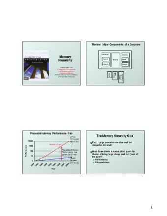
Motivation • Most applications in a single processor runs at only 10- 20% of the processor peak • Most of the single processor performance loss is in the memory system – Moving data takes much longer than arithmetic and logic • Parallel computing with low single machine performance is not good enough. • Understand high performance computing and cost in a single machine setting • Review of cache/memory hierarchy 2
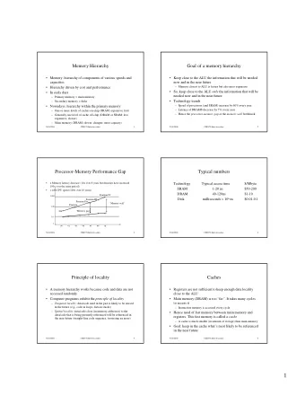
Typical Memory Hierarchy On-Chip Components Control Third- Level Secondary Main Cache Instr Second- Cache Memory Memory Level (SRAM) (Disk Datapath (DRAM) RegFile Cache Or Flash) Cache Data (SRAM) Speed (cycles): ½’s 1’s 10’s 100’s 1,000,000’s Size (bytes): 100’s 10K’s M’s G’s T’s Cost/bit: highest lowest Principle of locality + memory hierarchy presents programmer with • ≈ as much memory as is available in the cheapest technology at the ≈ speed offered by the fastest technology 3
Idealized Uniprocessor Model Processor names bytes, words, etc. in its address space • – These represent integers, floats, pointers, arrays, etc. Operations include • – Read and write into very fast memory called registers – Arithmetic and other logical operations on registers Order specified by program • – Read returns the most recently written data – Compiler and architecture translate high level expressions into “obvious” lower level instructions Read address(B) to R1 Read address(C) to R2 A = B + C Þ R3 = R1 + R2 Write R3 to Address(A) – Hardware executes instructions in order specified by compiler Idealized Cost • – Each operation has roughly the same cost (read, write, add, multiply, etc.) 4
Uniprocessors in the Real World • Real processors have – registers and caches • small amounts of fast memory • store values of recently used or nearby data • different memory ops can have very different costs – parallelism • multiple “functional units” that can run in parallel • different orders, instruction mixes have different costs – pipelining • a form of parallelism, like an assembly line in a factory • Why is this your problem? • In theory, compilers and hardware “understand” all this and can optimize your program; in practice they don’t. • They won’t know about a different algorithm that might be a much better “match” to the processor 5
Memory Hierarchy Most programs have a high degree of locality in their accesses • – spatial locality: accessing things nearby previous accesses – temporal locality: reusing an item that was previously accessed Memory hierarchy tries to exploit locality to improve average • processor control Second Secondary Main Tertiary level storage memory storage cache (Disk) datapath (DRAM) (Disk/Tape) (SRAM) on-chip registers cache Speed 1ns 10ns 100ns 1-10ms 10sec Size KB MB GB TB PB 6
Review: Cache in Modern Computer Architecture Memory Processor Input Control Program Cache Datapath Address Bytes PC Write Registers Data Data Arithmetic & Logic Unit Read Output (ALU) Data Processor-Memory Interface I/O-Memory Interfaces 7
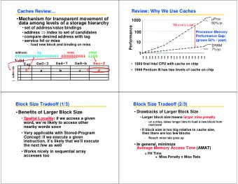
Cache Basics • Cache is fast (expensive) memory which keeps copy of data in main memory; it is hidden from software – Simplest example: data at memory address xxxxx1101 is stored at cache location 1101 • Memory data is divided into blocks – Cache access memory by a block (cache line) – Cache line length: # of bytes loaded together in one entry • Cache is divided by the number of sets – A cache block can be hosted in one set. • Cache hit: in-cache memory access—cheap • Cache miss: Need to access next, slower level of cache 8
Memory Block-addressing example address 8 address 8 address 8 00000 Byte 00000 0 0 00000 00001 00001 1 00001 Word 00010 00010 2 00010 00011 00011 3 00011 8-Byte 00100 00100 4 00100 Block 00101 00101 5 00101 00110 00110 6 00110 00111 00111 7 00111 01000 01000 1 0 01000 01001 01001 1 01001 01010 01010 2 01010 01011 01011 3 01011 01100 01100 4 01100 01101 01101 5 01101 01110 01110 6 01110 01111 01111 7 01111 10000 10000 2 0 10000 10001 10001 1 10001 10010 10010 2 10010 10011 10011 3 10011 10100 10100 4 10100 10101 10101 5 10101 10110 10110 6 10110 10111 10111 7 10111 11000 11000 3 0 11000 11001 11001 1 11001 11010 11010 11010 2 11011 11011 3 11011 11100 11100 4 11100 11101 11101 5 11101 11110 11110 6 11110 11111 11111 7 11111 2 LSBs are 0 3 LSBs are 0 Block # 10/4/17 9 Byte o ff set in block
Processor Address Fields used by Cache Controller • Block Offset: Byte address within block – B is number of bytes per block • Set Index: Selects which set. S is the number of sets • Tag: Remaining portion of processor address Processor Address Set Index Block offset Tag • Size of Tag = Address size – log(S) – log(B) Cache Size C = Associativity N × # of Set S × Cache Block Size B Example: Cache size 16K. 8 bytes as a block. à 2K blocks à If N=1, S=2K using 11 bits. Associativity N represents # items that can be held per set 10
Block number aliasing example 12-bit memory addresses, 16 Byte blocks Block # Block # mod 8 Block # mod 2 82 010100100000 2 010100100000 0 010100100000 83 010100110000 3 010100110000 1 010100110000 84 010101000000 4 010101000000 0 010101000000 85 010101010000 5 010101010000 1 010101010000 86 010101100000 6 010101100000 0 010101100000 87 010101110000 7 010101110000 1 010101110000 88 010110000000 0 010110000000 0 010110000000 89 010110010000 1 010110010000 1 010110010000 90 010110100000 2 010110100000 0 010110100000 91 010110110000 3 010110110000 1 010110110000 1-bit set index 3-bit set index 10/4/17 11
Direct-Mapped Cache: N=1. S=Number of Blocks=2 10 • 4byte blocks, cache size = 1K words (or 4KB) Byte offset 31 30 . . . 13 12 11 . . . 2 1 0 Tag 20 10 Data Valid bit Hit Index Read ensures Index Valid Tag Data data something 0 from useful in 1 2 cache cache for . instead this index . . of 1021 1022 memory Compare 1023 if a Hit Tag with 32 20 upper part of Comparator Address to see if a Hit Cache Size C = Associativity N × # of Set S × Cache Block Size B 12
Cache Organizations Cache Size C = N × # of Set S × Size B Associativity N represents # items that can be held per set • “Fully Associative”: Block can go anywhere – N= number of blocks. S=1 • “Direct Mapped”: Block goes one place – N=1. S= cache capacity in terms of number of blocks • “N-way Set Associative”: N places for a block Block ID Block ID
Four-Way Set-Associative Cache • 2 8 = 256 sets each with four ways (each with one block) Byte offset 31 30 . . . 13 12 11 . . . 2 1 0 Set Index Tag 22 8 Index V Tag Data V Tag Data V Tag Data V Tag Data 0 0 0 0 1 1 1 1 Way 0 Way 1 Way 2 Way 3 2 2 2 2 . . . . . . . . . . . . 253 253 253 253 254 254 254 254 255 255 255 255 32 4x1 select 14 Hit Data
How to find if a data address in cache? 0b means binary number • Assume block size 8 bytes à last 3 bits of address are offset. • Set index 2 bits. • Given address 0b1001011, where to find this item from cache? 15
How to find if a data address in cache? 0b means binary number • Assume block size 8 bytes à last 3 bits of address are offset. • Set index 2 bits. • 0b1001011 à Block number 0b1001. • Set index 2 bits (mod 4) • Set number à 0b01. • Tag = 0b10. • If directory based cache, only one block in set #1. • If 4 ways, there could be 4 blocks in set #1. • Use tag 0b10 to compare what is in the set. 16
Cache Replacement Policies Random Replacement • – Hardware randomly selects a cache evict Least-Recently Used • – Hardware keeps track of access history – Replace the entry that has not been used for the longest time – For 2-way set-associative cache, need one bit for LRU replacement Example of a Simple “Pseudo” LRU Implementation • – Assume 64 Fully Associative entries – Hardware replacement pointer points to one cache entry – Whenever access is made to the entry the pointer points to: • Move the pointer to the next entry – Otherwise: do not move the pointer – (example of “not-most-recently used” replacement policy) Entry 0 Entry 1 Replacement : Pointer 17 Entry 63
Handling Data Writing • Store instructions write to memory, changing values • Need to make sure cache and memory have same values on writes: 2 policies – 1) Write-through policy: write cache and write through the cache to memory • Every write eventually gets to memory • Too slow, so include Write Buffer to allow processor to continue once data in Buffer • Buffer updates memory in parallel to processor – 2) Write-back policy 18
Write-Through Processor Cache • Write both values in 32-bit 32-bit cache and in memory Address Data • Write buffer stops CPU Cache from stalling if memory cannot keep up 12 252 • Write buffer may have 99 1022 Write 7 131 multiple entries to Buffer 20 2041 absorb bursts of writes Addr Data • What if store misses in 32-bit 32-bit cache? Address Data Memory 19
Recommend
More recommend
Explore More Topics
Stay informed with curated content and fresh updates.


