Memory Hierarchy Motivation, Definitions, Four Questions about - PowerPoint PPT Presentation
Memory Hierarchy Motivation, Definitions, Four Questions about Memory Hierarchy Soner Onder Michigan Technological University Randy Katz & David A. Patterson University of California, Berkeley Levels in a memory hierarchy 2 Basic
Memory Hierarchy— Motivation, Definitions, Four Questions about Memory Hierarchy Soner Onder Michigan Technological University Randy Katz & David A. Patterson University of California, Berkeley
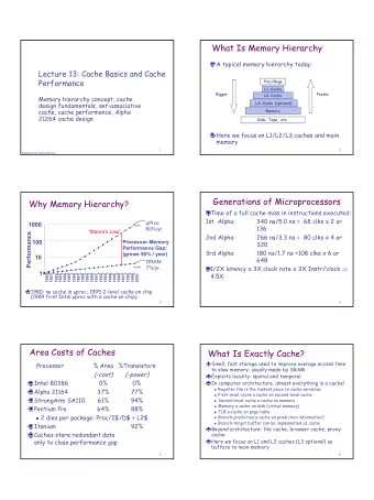
Levels in a memory hierarchy 2
Basic idea 3 Data block Tag Cache Memory Memory address =?
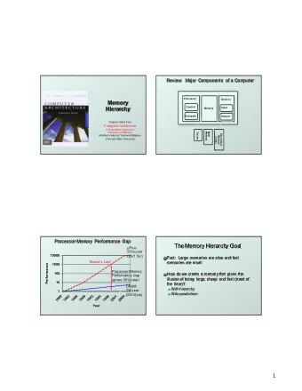
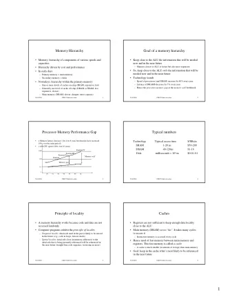
Who Cares about Memory Hierarchy? 4 1980: no cache in µproc; 1995 2-level cache, 60% trans. on Alpha 21164 µproc
General Principles 5 Locality Temporal Locality : referenced again soon Spatial Locality : nearby items referenced soon Locality + smaller HW is faster = memory hierarchy Levels : each smaller, faster, more expensive/byte than level below Inclusive : data found in top also found in the bottom Definitions Upper is closer to processor Block : minimum unit that present or not in upper level Address = Block frame address + block offset address Hit time : time to access upper level, including hit determination
Cache Measures 6 Hit rate : fraction found in that level So high that usually talk about Miss rate Miss rate fallacy: as MIPS to CPU performance, miss rate to average memory access time in memory Average memory-access time = Hit time + Miss rate x Miss penalty (ns or clocks) Miss penalty : time to replace a block from lower level, including time to replace in CPU access time : time to lower level = ƒ(lower level latency) transfer time : time to transfer block = ƒ(BW upper & lower, block size)
Block Size vs. Cache Measures 7 Increasing Block Size generally increases Miss Penalty Miss Miss Avg. X = Penalty Rate Memory Access Time Block Size Block Size Block Size
Implications For CPU 8 Fast hit check since every memory access Hit is the common case Unpredictable memory access time 10s of clock cycles: wait 1000s of clock cycles: Interrupt & switch & do something else New style: multithreaded execution How handle miss (10s => HW, 1000s => SW)?
Four Questions for Memory Hierarchy Designers 9 Q1: Where can a block be placed in the upper level? (Block placement) Q2: How is a block found if it is in the upper level? (Block identification) Q3: Which block should be replaced on a miss? (Block replacement) Q4: What happens on a write? (Write strategy)
Q1: Where can a block be placed in the upper level? 10 Block 12 placed in 8 block cache: Fully associative, direct mapped, 2-way set associative Set A. Mapping = Block Number Modulo Number Sets
Q2: How Is a Block Found If It Is in the Upper Level? 11 Tag on each block No need to check index or block offset Increasing associativity shrinks index, expands tag FA: No index DM: Large index
Q3: Which Block Should be Replaced on a Miss? 12 Easy for Direct Mapped S.A. or F.A.: Random (large associativities) LRU (smaller associativities) Associativity: 2-way 4-way 8-way Size LRU Random LRU Random LRU Random 16 KB 5.18% 5.69% 4.67% 5.29% 4.39% 4.96% 64 KB 1.88% 2.01% 1.54% 1.66% 1.39% 1.53% 256 KB 1.15% 1.17% 1.13% 1.13% 1.12% 1.12%
Q4: What Happens on a Write? 13 Write through: The information is written to both the block in the cache and to the block in the lower-level memory. Write back: The information is written only to the block in the cache. The modified cache block is written to main memory only when it is replaced. is block clean or dirty? Pros and Cons of each: WT: read misses cannot result in writes (because of replacements) WB: no writes of repeated writes WT always combined with write buffers so that don’t wait for lower level memory
Example: 21064 Data Cache 14 Index = 8 bits: 256 blocks = 8192/(32x1) Direct Mapped
Writes in Alpha 21064 15 No write merging vs. write merging in write buffer 4 entry, 4 word 16 sequential writes in a row
Structural Hazard: Instruction and Data? 16 Size Instruction Cache Data Cache Unified Cache 1 KB 3.06% 24.61% 13.34% 2 KB 2.26% 20.57% 9.78% 4 KB 1.78% 15.94% 7.24% 8 KB 1.10% 10.19% 4.57% 16 KB 0.64% 6.47% 2.87% 32 KB 0.39% 4.82% 1.99% 64 KB 0.15% 3.77% 1.35% 128 KB 0.02% 2.88% 0.95% Relative weighting of instruction vs. data access
2-way Set Associative, Address to Select Word 17 Two sets of Address tags and data RAM 2:1 Mux for the way Use address bits to select correct Data RAM
Cache Performance 18 CPU time = (CPU execution clock cycles + Memory stall clock cycles) x clock cycle time Memory stall clock cycles = (Reads x Read miss rate x Read miss penalty + Writes x Write miss rate x Write miss penalty) Memory stall clock cycles = Memory accesses x Miss rate x Miss penalty
Cache Performance 19 CPUtime = IC x (CPI execution + Mem accesses per instruction x Miss rate x Miss penalty) x Clock cycle time Misses per instruction = Memory accesses per instruction x Miss rate CPUtime = IC x (CPI execution + Misses per instruction x Miss penalty) x Clock cycle time
Improving Cache Performance 20 Average memory-access time = Hit time + Miss rate x Miss penalty (ns or clocks) Improve performance by: 1. Reduce the miss rate, 2. Reduce the miss penalty, or 3. Reduce the time to hit in the cache.
Summary 21 CPU-Memory gap is major performance obstacle for performance, HW and SW Take advantage of program behavior: locality Time of program still only reliable performance measure 4Qs of memory hierarchy
Recommend
More recommend
Explore More Topics
Stay informed with curated content and fresh updates.

