Analog Integrated Circuits Fundamental Building Blocks Fundamental - PowerPoint PPT Presentation
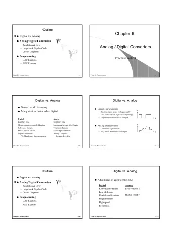
Analog Integrated Circuits Fundamental Building Blocks Fundamental Building Blocks Basic OTA/Opamp architectures Faculty of Electronics Telecommunications and Information Technology Information Technology Gabor Csipkes Bases of Electronics
Analog Integrated Circuits Fundamental Building Blocks Fundamental Building Blocks Basic OTA/Opamp architectures Faculty of Electronics Telecommunications and Information Technology Information Technology Gabor Csipkes Bases of Electronics Department
Outline definition of the OTA/opamp cascade of amplifier stages – the general opamp architecture the uncompensated Miller opamp – small signal model at low and high frequencies the uncompensated Miller opamp – small signal model at low and high frequencies step response of a second order system with unity feedback the two stage opamp with Miller compensation – models and parameters sizing algorithm for the two stage Miller opamp the telescopic opamp – voltage budget, models and parameters sizing algorithm of the telescopic opamp the folded cascode opamp – small signal low and high frequency model sizing algorithm for the folded cascode opamp Analog Integrated Circuits – Fundamental building blocks – Basic OTA/Opamp architectures 2
The ideal opamp - definitions ideal opamp = a differential input, voltage controlled voltage source with very large open loop gain the ideal gain is frequency independent, but real gain can be modeled with a set of poles and zeros → typically low pass behavior very large input resistance and near zero output resistance opamps with strictly capacitive loads can have large output resistance → Operational Transconductance Amplifiers (OTA) often also called opamp the output may be single ended (referenced to ground) or differential single or symmetrical supply voltages V a V V out Analog Integrated Circuits – Fundamental building blocks – Basic OTA/Opamp architectures 3
The opamp – a cascade of elementary stages the typical opamp architecture → a differential amplifier followed by a high gain inverting stage and a voltage follower for low output impedance the voltage follower may be missing if the load is known to be strictly capacitive frequency compensation for closed loop stability probably required (more on this later) frequency compensation for closed loop stability probably required (more on this later) elementary amplifier stages → subsequent V -I and I-V conversions most simple form → the two stage opamp V-I I-V I-V I-V cascade of elementary stages V-I Analog Integrated Circuits – Fundamental building blocks – Basic OTA/Opamp architectures 4
The two stage or Miller opamp Analog Integrated Circuits – Fundamental building blocks – Basic OTA/Opamp architectures 5
The two stage opamp the small signal low frequency model with two equivalent stages no capacitive effects → low frequency or DC voltage gain each stage can be analyzed individually → G m and R out specific to each configuration V G G g g m m 1 1 m m 1,2 1,2 a G R G R R r || r 0 m 1 out 1 m 2 out 2 out 1 DS 2 DS 4 a a G g 1 2 m 2 m 6 R r || r out 2 DS 6 DS 7 Analog Integrated Circuits – Fundamental building blocks – Basic OTA/Opamp architectures 6
The two stage opamp the small signal high frequency model → consider load and parasitic capacitances C C C 1 2 GD 1,2 C C C C C 3 GS 3 GS 4 DB 1 DB 3 V V C C C C 4 GD 4 C C C C 5 GS 6 DB 2 DB 4 C C 6 GD 6 C C C C C 7 L DB 6 DB 7 L a a s ( ) 0 1 1 sR sR C C 1 1 sR sR C C out out 1 1 5 5 out out 2 2 7 7 The frequency response is dominated by C 5 and C 7 due to the large R out 1 and R out 2 ! Analog Integrated Circuits – Fundamental building blocks – Basic OTA/Opamp architectures 7
The two stage opamp – with negative feedback the closed loop model of an opamp with negative feedback a a s ( ) 0 a s ( ) A s ( ) s s 1 1 1 a s ( ) r p 1 p 2 a 0 1 a r p 1 p 2 0 a s ( ) 1 a r A s ( ) 0 The closed loop gain: 1 a s ( ) r 2 s s 1 a r p 1 p 2 p 1 p 2 0 2 A A The standard form of a second order transfer function: The standard form of a second order transfer function: A s A s ( ) ( ) 0 0 n n (DC gain A 0 , resonant frequency ω n and damping factor ξ ) 2 2 s 2 s n n a 1 p 1 p 2 A 0 ; 1 a r ; 0 n p 1 p 2 0 1 a r r 2 1 a r 0 p 1 p 2 0 Analog Integrated Circuits – Fundamental building blocks – Basic OTA/Opamp architectures 8
Frequency response of a second order system the effect of the feedback transmittance r on the magnitude response 1 A 0 r A 0 decreases with r Overshoot of the frequency response at ω n → complex poles → under damped step response worst case stability for unity gain ( r =1 and A 0 =1) → lowest ξ for given a 0 , ω p 1 and ω p 2 Analog Integrated Circuits – Fundamental building blocks – Basic OTA/Opamp architectures 9
Step response for unity gain feedback A s ( ) L 1 V ( ) t the time domain step response is calculated as out s damping of the oscillation amplitude depends on ξ typically, if poles ω p 1 and ω p 2 are close to each other ξ <1 → under damped system with fading oscillations of the step response fading oscillations of the step response n t 2 1 e 2 V ( ) t 1 sin 1 t arctan out n 2 1 fading exponential fading exponential oscillations with the period oscillations with the period envelope depending on ω n and ξ since the sin function varies between - 1 and 1 → time domain overshoot around the unit step → the overshoot and number of cycles until settling increases with a smaller ξ Analog Integrated Circuits – Fundamental building blocks – Basic OTA/Opamp architectures 10
Step response for unity gain feedback step response of the two stage opamp in unity gain feedback configuration optimal optimal response the circuit is unusable as amplifier for small ξ due to the very long settling time the response stability depends on the phase margin ( m φ ) → optimal response for m φ =65° Analog Integrated Circuits – Fundamental building blocks – Basic OTA/Opamp architectures 11
Stability and phase margin a s ( ) A s ( ) closed loop gain for unity feedback: What if denominator is 0 ??? 1 a s ( ) a s ( ) 1 the closed loop gain approaches ∞ → even for no input any perturbation is amplified with under damped transients → sustained oscillations occur, feedback turns positive and with under damped transients → sustained oscillations occur, feedback turns positive and system becomes unstable a j ( ) 1 Barkhausen's stability criteria: a j ( ) 180 a 0 solve for ω f 1 0 dB 1 j 1 j p p 1 1 p p 2 2 m 180 a j odB 180 arctan 0 dB arctan 0 dB p 1 p 2 Analog Integrated Circuits – Fundamental building blocks – Basic OTA/Opamp architectures 12
Pole locations and phase margin the relation between pole frequencies and f 0 dB defines m φ and the stability of the step response This is what we need ! we need ! f f f f f f p 2 0 dB p 2 0 dB p 2 0 dB m 45 m 45 m 45 Analog Integrated Circuits – Fundamental building blocks – Basic OTA/Opamp architectures 13
Frequency compensation need f p 2 > f 0 dB so that m φ >45° → impossible to achieve by simply cascading a differential amplifier and a common source inverting amplifier Typically: 1 f p p 1 1 R R R R 2 2 R R C C out 1 out 2 out 1 5 C C 1 7 5 f p 2 2 R C out 2 7 f p 1 and f p 2 are close to each other !!! We need to manipulate pole locations to separate f p 1 and f p 2 → → frequency compensation Analog Integrated Circuits – Fundamental building blocks – Basic OTA/Opamp architectures 14
Recommend
More recommend
Explore More Topics
Stay informed with curated content and fresh updates.
