8086 Chipset Systems Design & Programming CMPE 310 8086/88 - PowerPoint PPT Presentation
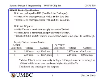
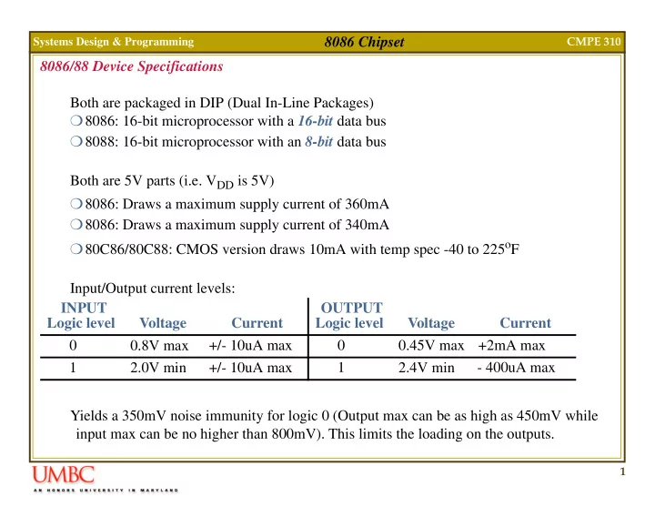
8086 Chipset Systems Design & Programming CMPE 310 8086/88 Device Specifications Both are packaged in DIP (Dual In-Line Packages) 8086: 16-bit microprocessor with a 16-bit data bus 8088: 16-bit microprocessor with an 8-bit data bus
8086 Chipset Systems Design & Programming CMPE 310 8086/88 Device Specifications Both are packaged in DIP (Dual In-Line Packages) � 8086: 16-bit microprocessor with a 16-bit data bus � 8088: 16-bit microprocessor with an 8-bit data bus Both are 5V parts (i.e. V DD is 5V) � 8086: Draws a maximum supply current of 360mA � 8086: Draws a maximum supply current of 340mA � 80C86/80C88: CMOS version draws 10mA with temp spec -40 to 225 o F Input/Output current levels: INPUT OUTPUT Logic level Voltage Current Logic level Voltage Current 0 0.8V max +/- 10uA max 0 0.45V max +2mA max 1 2.0V min +/- 10uA max 1 2.4V min - 400uA max Yields a 350mV noise immunity for logic 0 (Output max can be as high as 450mV while input max can be no higher than 800mV). This limits the loading on the outputs. 1
8086 Chipset Systems Design & Programming CMPE 310 8086/88 Pinout 8086 CPU MIN MODE (MAX MODE) VCC GND 40 1 AD15 AD14 2 39 A16/S3 AD13 3 38 A17/S4 AD12 4 37 A18/S5 AD11 5 36 A19/S6 AD10 6 35 BHE/S7 AD9 7 34 MN/MX AD8 8 33 RD AD7 9 32 Hold ( RQ/GT0 ) AD6 10 31 HLDA ( RQ/GT1 ) AD5 11 30 WR ( LOCK ) AD4 12 29 M/IO ( S2 ) AD3 13 28 DT/R ( S1 ) AD2 14 27 DEN ( S0 ) AD1 15 26 ALE ( QS0 ) AD0 16 25 INTA ( QS1 ) NMI 17 24 TEST INTR 18 23 READY CLK 19 22 RESET GND 20 21 2
8086 Chipset Systems Design & Programming CMPE 310 8086/88 Pinout � AD15-AD0 Multiplexed address(ALE=1)/data bus(ALE=0). � A19/S6-A16/S3 (multiplexed) High order 4 bits of the 20-bit address OR status bits S6-S3. � M/IO Indicates if address is a Memory or IO address. � RD When 0, data bus is driven by memory or an I/O device. � WR Microprocessor is driving data bus to memory or an I/O device. When 0, data bus con- tains valid data. � ALE (Address latch enable) When 1, address data bus contains a memory or I/O address. � DT/R (Data Transmit/Receive) Data bus is transmitting/receiving data. � DEN (Data bus Enable) Activates external data bus buffers. 3
8086 Chipset Systems Design & Programming CMPE 310 8086/88 Pinout � S7, S6, S5, S4, S3, S2, S1, S0 S7 : Logic 1, S6: Logic 0. S5 : Indicates condition of IF flag bits. S4-S3 : Indicate which segment is accessed during current bus cycle: S4 S3 Function 0 0 Extra segment 0 1 Stack segment 1 0 Code or no segment 1 1 Data segment S2 , S1 , S0 : Indicate function of current bus cycle (decoded by 8288). Function Function S2 S1 S0 S2 S1 S0 0 0 0 1 0 0 Interrupt Ack Opcode Fetch 0 0 1 1 0 1 I/O Read Memory Read 0 1 0 1 1 0 I/O Write Memory Write 0 1 1 1 1 1 Halt Passive 4
8086 Chipset Systems Design & Programming CMPE 310 8086/88 Pinout � INTR When 1 and IF=1, microprocessor prepares to service interrupt. INTA becomes active after current instruction completes. � INTA Interrupt Acknowledge generated by the microprocessor in response to INTR. Causes the interrupt vector to be put onto the data bus. � NMI Non-maskable interrupt. Similar to INTR except IF flag bit is not consulted and inter- rupt is vector 2. � CLK Clock input must have a duty cycle of 33% (high for 1/3 and low for 2/3s) � VCC/GND Power supply (5V) and GND (0V) � MN/MX Select minimum (5V) or maximum mode (0V) of operation. 5
8086 Chipset Systems Design & Programming CMPE 310 8086/88 Pinout � BHE Bus High Enable. Enables the most significant data bus bits (D 15 -D 8 ) during a read or write operation. � READY Used to insert wait states (controlled by memory and IO for reads/writes) into the microprocessor. � RESET Microprocessor resets if this pin is held high for 4 clock periods. Instruction execution begins at FFFF0H and IF flag is cleared. � TEST An input that is tested by the WAIT instruction. Commonly connected to the 8087 coprocessor. � HOLD Requests a direct memory access (DMA). When 1, microprocessor stops and places address, data and control bus in high-impedance state. � HLDA (Hold Acknowledge) Indicates that the microprocessor has entered the hold state. 6
8086 Chipset Systems Design & Programming CMPE 310 8086/88 Pinout � RO/GT1 and RO/GT0 Request/grant pins request/grant direct memory accesses (DMA) during maximum mode operation. � LOCK Lock output is used to lock peripherals off the system. Activated by using the LOCK: prefix on any instruction. � QS1 and QS0 The queue status bits show status of internal instruction queue. Provided for access by the numeric coprocessor (8087). 7
8086 Chipset Systems Design & Programming CMPE 310 8284A Clock Generator � Clock generation � RESET synchronization � READY synchronization � Peripheral clock signal Connection of the 8284 and the 8086. 18 1 CSYNC X1 Crystal 2 17 OSC 3 16 X2 8284A 15MHz 4 15 5 14 8086 F/C 6 13 7 12 CLK 8 11 9 10 RESET CLK RESET 8
8086 Chipset Systems Design & Programming CMPE 310 8284A Clock Generator VCC CSYNC 18 RES 1 RESET D Q X1 PCLK 17 2 X2 AEN1 16 3 Schmitt 8284A ASYNC RDY1 15 trigger 4 EFI READY 14 5 X1 F/C RDY2 13 6 OSC XTAL OSC AEN2 12 7 (EFI input X2 OSC RES CLK 11 8 to other RESET GND 10 9 8284As) div- div- F/C by-3 by-2 2-to-1 mux PCLK cnter cnter +3 +2 EFI CSYNC RDY1 CLK AEN1 READY RDY2 D Q D Q AEN2 ASYNC 9
8086 Chipset Systems Design & Programming CMPE 310 8284A Clock Generator Clock generation Crystal is connected to X1 and X2. XTAL OSC generates square wave signal at crystal's frequency which feeds: � An inverting buffer (output OSC) which is used to drive the EFI input of other 8284As. � 2-to-1 MUX F/C selects XTAL or EFI external input. The MUX drives a divide-by-3 counter (15MHz to 5MHz). This drives: � The READY flipflop (READY synchronization). � A second divide-by-2 counter (2.5MHz clk for peripheral components). � The RESET flipflop. � CLK which drives the 8086 CLK input. 10
8086 Chipset Systems Design & Programming CMPE 310 8284A Clock Generator RESET Negative edge-triggered flipflop applies the RESET signal to the 8086 on the falling edge. The 8086 samples the RESET pin on the rising edge. CSYNC: Used with multiple processors. 1 18 CSYNC X1 Crystal 2 17 OSC 3 16 X2 15MHz 8284A 4 15 +5V 5 14 8086 F/C Reset 6 13 switch 10K 7 12 CLK RES 8 11 9 10 10uF RESET CLK RESET RC = 10K*10uF ~= 100msec Correct reset timing requires that the RESET input to the microprocessor becomes a logic 1 NO LATER than 4 clocks after power up and stay high for at least 50 µ s. 11
8086 Chipset Systems Design & Programming CMPE 310 BUS Buffering and Latching Computer systems have three buses � Address � Data � Control The Address and Data bus are multiplexed (shared) due to pin limitations on the 8086. The ALE pin is used to control a set of latches. All signals MUST be buffered Buffered Latches for A 0 -A 15 . Control and A 16 -A 19 + BHE are buffered separately. Data bus buffers must be bi-directional buffers. In a 8086 system, the memory is designed with two banks High bank contains the higher order 8-bits and low bank the lower order 8-bits Data can be transferred as 8 bits from either bank or 16-bits from both BHE pin selects the high-order memory bank 12
8086 Chipset Systems Design & Programming CMPE 310 BUS Buffering and Latching BHE A 19 Buffer A 16 VCC GND A 15 Address Bus AD15 AD14 A16/S3 AD13 A17/S4 AD12 A 8 A18/S5 AD11 A 7 A19/S6 AD10 BHE/S7 AD9 MN/MX AD8 RD AD7 8086 CPU A 0 Hold AD6 G G HLDA AD5 Latches Latches WR AD4 D 15 M/IO AD3 DT/R AD2 BB DEN Data Bus AD1 G D ALE AD0 D 8 INTA NMI D 7 TEST INTR BB READY CLK RESET G D GND D 0 Buffer Control 13
8086 Chipset Systems Design & Programming CMPE 310 BUS Timing Writing � Dump address on address bus. � Dump data on data bus. � Issue a write (WR) and set M/IO to 1. One Bus Cycle T 2 T 3 T 1 T 4 CLK Address Valid Address Address/Data Address Data written to memory WR Simplified 8086 Write Bus Cycle 14
8086 Chipset Systems Design & Programming CMPE 310 BUS Timing Reading � Dump address on address bus. � Issue a read (RD) and set M/IO to 1. � Wait for memory access cycle. One Bus Cycle T 2 T 3 T 1 T 4 CLK Address Valid Address Address/Data Address Data from memory RD Simplified 8086 Read Bus Cycle 15
8086 Chipset Systems Design & Programming CMPE 310 BUS Timing Read Bus Timing: 800ns 200ns T w T 2 T 3 T 1 T 4 CLK A 19 -A 16 /S 6 -S 3 A 19 -A 16 S 7 -S 3 Float Float AD 15 -AD 0 AD 15 -AD 0 Data In M/IO Address setup Data setup ALE DT/R RD DEN READY Bus Timing for a Read Operation 16
8086 Chipset Systems Design & Programming CMPE 310 BUS Timing During T 1 : � The address is placed on the Address/Data bus. � Control signals M/IO, ALE and DT/R specify memory or I/O, latch the address onto the address bus and set the direction of data transfer on data bus. During T 2 : � 8086 issues the RD or WR signal, DEN, and, for a write, the data. � DEN enables the memory or I/O device to receive the data for writes and the 8086 to receive the data for reads. During T 3 : � This cycle is provided to allow memory to access data. � READY is sampled at the end of T 2 . If low, T 3 becomes a wait state. Otherwise, the data bus is sampled at the end of T 3 . During T 4 : � All bus signals are deactivated, in preparation for next bus cycle. � Data is sampled for reads, writes occur for writes. 17
Recommend
More recommend
Explore More Topics
Stay informed with curated content and fresh updates.
