SYSC3601 Microprocessor Systems Unit 4: 8086/88 Hardware & Bus - PowerPoint PPT Presentation
SYSC3601 Microprocessor Systems Unit 4: 8086/88 Hardware & Bus Structure Topics/Reading Brey Chapter 9: Hardware specifications Pin-outs & pin functions 8274 Clock generator Bus buffering & latching Bus
SYSC3601 Microprocessor Systems Unit 4: 8086/88 Hardware & Bus Structure
Topics/Reading • Brey Chapter 9: Hardware specifications – Pin-outs & pin functions – 8274 Clock generator – Bus buffering & latching – Bus timing – Ready & the wait state – Minimum mode vs. maximum mode SYSC3601 2 Microprocessor Systems
8086/88 Hardware and Bus Structure • We will now focus on the 8086/88 hardware and pin functions – later we will review characteristics of other Intel µ P and the Motorola family. • Although these µ P’s are fairly old, they still are a good way to introduce the Intel family of microprocessors. • Both machines are 16-bit microprocessors. The 8088 has an 8-bit data bus and the 8086 has a 16-bit data bus. • Still used in embedded systems (cost < $1) SYSC3601 3 Microprocessor Systems
8086/88 Hardware and Bus Structure Abstract diagram showing data flow in/out of µ P SYSC3601 4 Microprocessor Systems
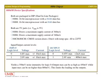
8086/88 Hardware and Bus Structure • General Characteristics – Power: • 8086 +5V ± 10%, 360mA (80C86 10mA) • 8088 +5V ± 10%, 340mA (80C86 10mA) – Temp: • 32ºF - 180ºF (not suitable for outdoors) • CMOS version -40ºF - 255ºF (MIL spec) – Clock Frequency: • normally 5MHz. SDK86: 2.5MHz or 5MHz. – DC characteristics • Must understand V-A characteristics of I/O pins in order to connect to the outside world. (next slide) SYSC3601 5 Microprocessor Systems
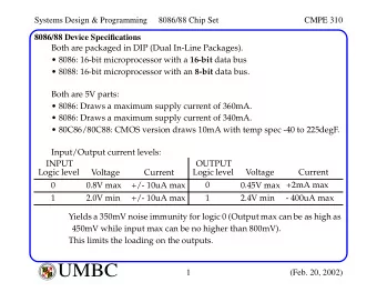
8086/88 Hardware and Bus Structure – Input characteristics • compatible with standard logic-level components – logic 0: 0.8V max, 10 µ A max – logic 1: 2.0V min, 10 µ A max • The input current is very small – gates of MOSFETs, so current represents leakage. – Output characteristics • logic 1 voltage level is compatible with most logic families, but logic 0 is not . (Most logic families have logic 0 max 0.4V) – logic 0: 0.45V max, ± 2.0 mA max – logic 1: 2.0V min, ± 400 µ A max • No more than 10 loads per output without buffering. • If more than 10 loads are attached to any bus pin, then the entire 8086/8088 must be buffered. SYSC3601 6 Microprocessor Systems
8086/8088 Pin assignments & functions 8086/8088 DIP pin assignments (max mode in brackets) SYSC3601 7 Microprocessor Systems
8086/8088 Pin assignments & functions • Both the 8086 and the 8088 are 40-pin Dual In-line Package (DIP) chips. • 8086 – 16-bit µ P and a 16-bit data bus • 8088 – 16-bit µ P and a 8-bit data bus • 8086 has M/IO, 8088 has IO/M – See text Fig 9-1. Note that on 8088, IO/M should be IO/M • Pin 34 is also different: 8086 BHE/S7, 8088 has SSO SYSC3601 8 Microprocessor Systems
8086/8088 Pin assignments & functions • AD 15 - AD 0 – Multiplexed address/data bus. – lines carry address bits A 15 - A 0 whenever ALE (Address Latch Enable) is logic 1. – lines carry data bits D 15 - D 0 whenever ALE is logic 0. – Note: 8088 only multiplexes D 7 - D 0 because it uses an 8-bit data bus. • A 19 /S 6 - A 16 /S 3 – multiplexed address/status bits. – lines carry address bits A 19 - A 16 whenever ALE is logic 1. – lines carry status bits S 6 - S 3 whenever ALE is logic 0. SYSC3601 9 Microprocessor Systems
8086/8088 Pin assignments & functions • S 6 always logic zero (not used). • S 5 matches state of I flag bit (interrupt) • S 4 &S 3 reports segment being accessed during current bus cycle: S 4 S 3 Function 0 0 Extra Segment (ES) 0 1 Stack Segment (SS) 1 0 Code Segment (CS) 1 1 Data Segment (DS) • Note: These status lines could be decoded/latched to address four separate 1M banks of memory. (Split I/D) SYSC3601 10 Microprocessor Systems
8086/8088 Pin assignments & functions • RD µ P is set to receive data when low • WR µ P is outputting data when low • M/IO (8086) indicates a memory address (‘1’), or an I/O address (‘0’). • DT/R Data transmit/receive. Data bus is transmitting (‘1’), or receiving (‘0’) (for controlling bi-directional bus drivers). • DEN Data bus enable – used to activate external buffers/transceivers. • BHE/S7 Bank high enable – used to enable D 15 - D 8 in an 8086 during a 16-bit read/write. – Multiplexed with S7, which is not used (always 1). – latched with ALE. SYSC3601 11 Microprocessor Systems
8086/8088 Pin assignments & functions • Pins to be discussed later: – READY: Used to insert wait states (controlled by memory and IO for reads/writes) into the microprocessor. – RESET: Microprocessor resets if this pin is held high for 4 clock periods. Instruction execution begins at FFFF0H and IF flag is cleared. – CLK: Provides clock signal to 8086 – HOLD: Requests a direct memory access (DMA). When 1, microprocessor stops and places address, data and control bus in high-impedance state. – HLDA (Hold Acknowledge): Indicates that the microprocessor has entered the hold state. RO/GT 1 and RO/GT 0 : Request/grant pins – request/grant direct memory accesses (DMA) during maximum mode operation. SYSC3601 12 Microprocessor Systems
8086/8088 Pin assignments & functions • Pins to be discussed later: – INTR: Used to request an interrupt – NMI: Used to request a non-maskable interrupt – INTA: Output to acknowledge an interrupt. – TEST: An input that is tested by the WAIT instruction. Commonly connected to the 8087 coprocessor. QS 1 and QS 0 : The queue status bits show status of – internal instruction queue. Provided for access by the numeric coprocessor (8087). – LOCK: Lock output is used to lock peripherals off the system. Activated by using the LOCK: prefix on any instruction. SYSC3601 13 Microprocessor Systems
8086/8088 Pin assignments & functions • Both the 8086 and the 8088 have two modes of operation: 1. Minimum Mode: connect MN/MX to +5V (directly). – similar to 8085 operation. – all control signals for memory and I/O are generated by the µ P. – (RD, M/IO, DT/R, DEN, ALE, INTA, WR, etc) 2. Maximum Mode: connect MN/MX to ground (directly). – dropped by Intel beginning with the 80286. – must use with co-processor (8087) present. – some control signals must be generated externally. – use with 8288 bus controller. SYSC3601 14 Microprocessor Systems
8288 Bus Controller (use when in MAX mode) 8086 8288 s 0 s 0 MRDC MWTC s 1 s 1 ctrl IORD s 2 s 2 Other ctrl IOWT signals 8288 Bus Controller INTA DT/R s 0-3 = state data from 8086 DEN ALE 8282 STB 8282 Tri-State Octal Latch OE STB=data strobe (admit new data) OE = output enable addr addr/data 8286 T 8286 Octal Bus Transceiver OE T=transmit data OE = output enable (in either dir) Some details omitted… We will see how to achieve buffering & demultiplexing using generic chips… SYSC3601 15 Microprocessor Systems
Decoding Bus Control Signal • In “max mode” use 8288 bus controller to generate MRDC,MWTC, IORC, IOWC. • In “min mode” (and for other processors) it is sometimes better to decode the available signals. SYSC3601 16 Microprocessor Systems
8284A Clock Generator • Used with 8086/88 to generate 1. clock signal (see next slide) 2. reset signal (see next slide) 3. ready signals (wait states) • Inputs: – F / C Frequency/crystal select. 1 external clock 0 crystal (X1-X2 provides timing). – CSYNC Only used with external clock, otherwise grounded. – RES Reset input pin. Generates RESET output. SYSC3601 17 Microprocessor Systems
8284A Clock Generator 10K pullup? 0.5mA sink. (debouncing!) SYSC3601 18 Microprocessor Systems
Bus Transfer Synchronization • Synchronous busses (eg. Motorola 6800/11/12) – Transfer times and synchronization are tied to the system clock. – No facility for varying bus timing. – Clock generators could be used to vary bus speed (for slower memory), but would slow entire µ P • Semi-synchronous busses – provide for “wait states” to be inserted into bus timing (eg. 8086). – Allows more flexibility in interfacing to slower memory or I/O. • Asynchronous busses (eg. Motorola 68000). – Requires extra bus signals for bus arbitration. – Requires “acknowlegement” signal from devices. – Requires bus time-out (watchdog). – Easier multiprocessor memory management. SYSC3601 19 Microprocessor Systems
Bus Timing • 8086 and 8088 bus cycles consume four system clock periods (T-states), T 1 , T 2 , T 3 and T 4 . • At 5MHz, each T-state is 200nS, therefore a bus cycle is 800nS. • Semi-synchronous bus control allows inserting of wait states (T w ), also 200nS, between T 3 and T 4 which allows access to slow memory and I/O devices – (Text says T w inserted between T 2 and T 3 , but the Intel manual says between T 3 and T 4 ). • Most processors are very similar in I/O and memory access operations. SYSC3601 20 Microprocessor Systems
Write Cycle data (FROM µ P) address SYSC3601 21 Microprocessor Systems
Read Cycle data (TO µ P) address SYSC3601 22 Microprocessor Systems
Recommend
More recommend
Explore More Topics
Stay informed with curated content and fresh updates.
