5. Simulate the n-bit modular adder/subtracter architecture The - PDF document
Summer School on Real-world Crypto and Privacy Hardware tutorial June 14, 2018, ibenik, Croatia Nele Mentens (KU Leuven) Pedro Maat Costa Massolino (Radboud University) TUTORIAL INSTRUCTIONS In this tutorial, we will design and simulate a
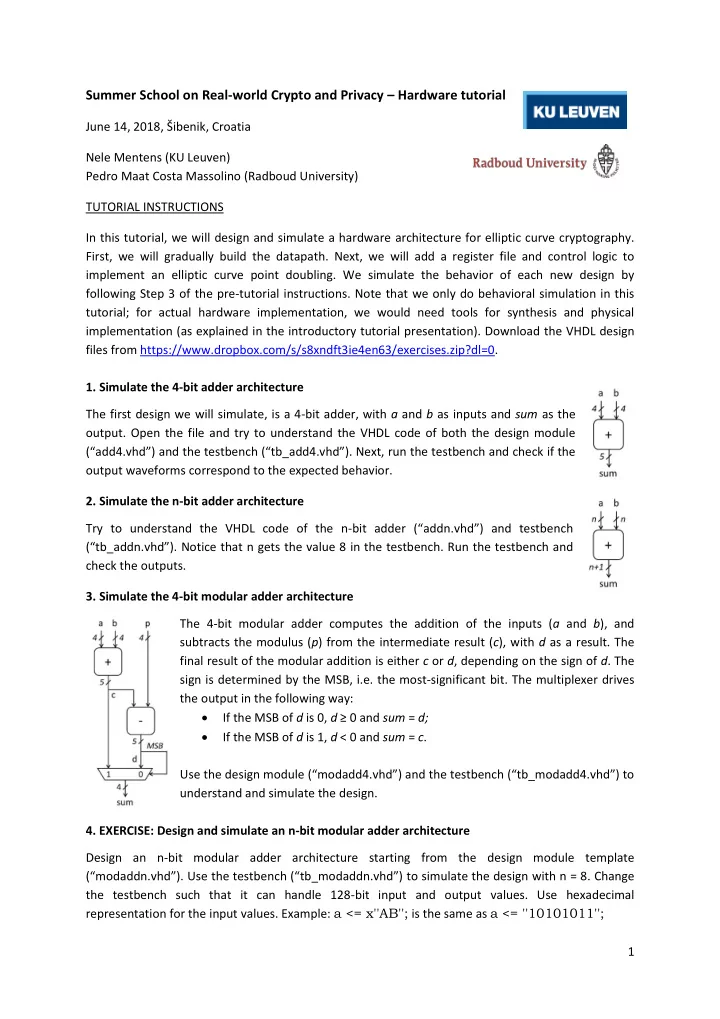
Summer School on Real-world Crypto and Privacy – Hardware tutorial June 14, 2018, Š ibenik, Croatia Nele Mentens (KU Leuven) Pedro Maat Costa Massolino (Radboud University) TUTORIAL INSTRUCTIONS In this tutorial, we will design and simulate a hardware architecture for elliptic curve cryptography. First, we will gradually build the datapath. Next, we will add a register file and control logic to implement an elliptic curve point doubling. We simulate the behavior of each new design by following Step 3 of the pre-tutorial instructions. Note that we only do behavioral simulation in this tutorial; for actual hardware implementation, we would need tools for synthesis and physical implementation (as explained in the introductory tutorial presentation). Download the VHDL design files from https://www.dropbox.com/s/s8xndft3ie4en63/exercises.zip?dl=0. 1. Simulate the 4-bit adder architecture The first design we will simulate, is a 4-bit adder, with a and b as inputs and sum as the output. Open the file and try to understand the VHDL code of both the design module ( “add4.vhd”) and the testbench (“tb_add4.vhd”). Next, run the testbench and check if the output waveforms correspond to the expected behavior. 2. Simulate the n-bit adder architecture Try to understand the VHDL code of the n- bit adder (“addn.vhd”) and testbench (“tb_addn.vhd”). Notice that n gets the value 8 in the testbench. Run the testbench and check the outputs. 3. Simulate the 4-bit modular adder architecture The 4-bit modular adder computes the addition of the inputs ( a and b ), and subtracts the modulus ( p ) from the intermediate result ( c ), with d as a result. The final result of the modular addition is either c or d , depending on the sign of d . The sign is determined by the MSB, i.e. the most-significant bit. The multiplexer drives the output in the following way: If the MSB of d is 0, d ≥ 0 and sum = d; If the MSB of d is 1, d < 0 and sum = c . Use the design module (“modadd4.vhd”) and the testbench (“tb_modadd4.vhd”) to understand and simulate the design. 4. EXERCISE: Design and simulate an n-bit modular adder architecture Design an n-bit modular adder architecture starting from the design module template (“modaddn.vhd”). Use the testbench (“tb_modaddn.vhd”) to simulate the design with n = 8. Change the testbench such that it can handle 128-bit input and output values. Use hexadecimal representation for the input values. Example: a <= x''AB''; is the same as a <= ''10101011''; 1
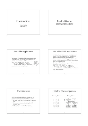
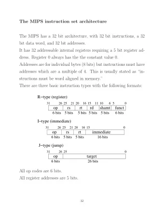
5. Simulate the n-bit modular adder/subtracter architecture The modular adder/subtracter performs either a modular addition (when the add/subtract signal, as , is 0) or a modular subtraction (when as is 1) on the inputs a and b with modulus p . Try to understand the architecture and the design file (“modaddsubn.vhd”). Simulate the behavior of the module using the testbench (“tb_modaddsubn.vhd”). We will use this module in the design of the elliptic curve point doubling. 6. Simulate the n-bit constant multiplier (multiplication by 5) This is a module that we will not use in the design of the elliptic curve point doubling, but it should be a good starting point for the following two exercises on n-bit modular multipliers. Try to understand the architecture and the design file ( “modaddn_mult5.vhd” ) and run the testbench ( “tb_modaddn_mult5.vhd” ). The architecture of the design module contains input registers to store a and p . New values are loaded when start = 1. The start signal also initiates a finite state machine (FSM) that interacts with a counter to make sure the modular addition is performed 5 times. 7. EXERCISE: Design and simulate an n-bit multiplier (by consecutive modular additions) and simulate the behavior Start from the design module template (“modaddn_mult.vhd”) and use the testbench (“tb_modaddn_mult.vhd”). The goal is to build a modular multiplier by consecutive modular additions of the multiplicand. Note that this is not an efficient way of implementing a modular multiplier, because it requires an impractical number of modular additions to be executed. 2
8. EXERCISE: Design and simulate an n-bit modular multiplier (through a left-to-right modular double-and-add algorithm) Start from the design module template (“modmultn.vhd”) and use the testbench (“tb_modmultn.vhd”). The architecture of the design module contains input registers to store a , b and p . The register to store b is also shiftable. When the shift input is active, the register shifts its content one position to the left (and shifts in a 0 on the right side). The registers are already present in the template design file. The FSM uses the left bit of b to determine the next step in the algorithm. First, draw the FSM and the hardware architecture. Then, design the architecture in VHDL. Finally, run the simulation to check if the product is as expected. 9. Simulate the 4*n-bit register file Use “regfile_4_n.vhd” and “tb_regfile_4_n.vhd”. Try to understand how the register file works and run the simulation. 3
10. EXERCISE: Design and simulate a point doubling architecture Design the hardware architecture for the n-bit point doubling operation given by the algorithm below (source: “Guide to Elliptic Curve Cryptography” by Hankerson et al ). Use the register file (which you will need to extend to a larger depth) and the modular multiplier and modular adder/subtracter. Create a new file and testbench called “point_double.vhd” and “tb_point_double.vhd”. Draw the architecture on a piece of paper first. 4
Recommend
More recommend
Explore More Topics
Stay informed with curated content and fresh updates.
![Problem 1 Design a Verilog 16-bit adder module module adder (A, B, sum); input [15:0] A, B;](https://c.sambuz.com/1025319/problem-1-design-a-verilog-16-bit-adder-module-module-s.webp)
