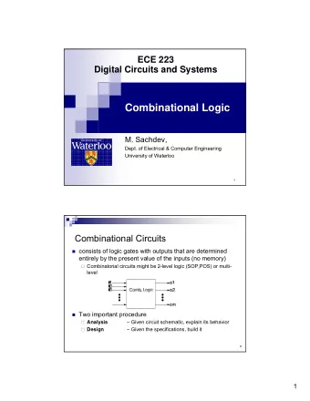
Combinatorial networks- II Digital Systems M 1 Adder Lets see the - PowerPoint PPT Presentation
Combinatorial networks- II Digital Systems M 1 Adder Lets see the truth table of a combinatorial network whose output values correspond to the numerical values of a 2-bit adder (Half Adder) ab Sum Carry 00 0
Combinatorial networks- II Digital Systems M 1
Adder • Let’s see the truth table of a combinatorial network whose output values correspond to the numerical values of a 2-bit adder (Half Adder) ab Sum Carry 00 0 0 a 01 1 0 Sum = a ⊕ b = a exor b Sum a Sum b 10 1 0 HA 11 0 1 Carry=ab b Carry Carry • Let’s see the truth table of a combinatorial network whose output values correspond to the numerical values of a 3-bit adder (Full Adder). Canonical synthesis SP Sum = !a!bc+!ab!c+a!b!c+abc=!a(!bc+b!c)+a(!b!c+bc) =!a(b exor c)+a!(b exor c) = a exor (b exor c) Carry = !abc+a!bc+ab!c+abc = c(a exor b) + ab(c+!c) = c(a exor b) + ab abc Sum Carry Sum Sum1 = a exor b Sum2 =a exor (b exor c) 000 0 0 a 001 1 0 HA HA Carry1=ab Carry2=c(a exor b) Full Adder 010 1 0 b 011 0 1 Carry 100 1 0 c 101 0 1 110 0 1 111 1 1 For the carry we have also C= !abc+a!bc+ab!c+abc = !abc+a!bc+ab!c+abc+abc+abc = ab(c+!c) + ac(b+!b) + bc(a+!a) = ab + ac + bc Added terms (idempotence) 2 (It could have been intuitively deduced since two 1’s are enough for generating a carry !!!)
Adder To add a binary number of n bit, n-1 FA e 1 HA must be used a 0 S 0 HA NB: Normally the integrated circuits provide 4 bit FAs. With C b 0 this network a new logical level (delay) is introduced for each couple of bit to be added. It must be remembered however that this is a combinatorial network which S 1 corresponds to a truth table which can be always FA a 1 C synthesised as a two levels b 1 network (minimum delay). In the 4 bit integrated FAs the carry is always generated with a two level network in order to S 2 accelerate the operations of the next level FA. FA a 2 C b 2 3
FA 4-bit 74X283 4
FA 8-bit 5
Carry Look Ahead I • With 4 bit full-adders a fast carry generator is implemented • Two carries are defined: carry generate (G) and carry propagate (P) Considering the sum of two binary numbers with A i and B i the bits in the i-th position we define G i • the logical product A i *B i (1 only if both bit are 1) and P i the logical sum A i or B i which if A i =1 or B i =1 produces arithmetically always a carry (C i+1 ) if there is a carry (C i of index i) • It follows that C i+1 =(G i or P i C i ) (G i =1 if A i =B i =1; P i C i =1 if A i or B i =1 and C i =1) (if G i =1 then P i C i has no infuence. If G i =0 and P i =1 then P i C i =C i since a carry is produced if there is a carry from the precious stage and one element of the addition is 1). Therefore we have (here symbols + indicate always or) C 1 =G 0 +P 0 C 0 C 2 =G 1 +P 1 C 1 = G 1 + P 1 (G 0 +P 0 C 0 )= G 1 + G 0 P 1 + C 0 P 0 P 1 etc. and then substituting C 4 = G 3 +G 2 P 3 +G 1 P 2 P 3 +G 0 P 1 P 2 P 3 +C 0 P 0 P 1 P 2 P 3 (carry of the 4 0h bit) Two level network (SP) Remember: a combinatorial network can be always implemented as a two level PS od SP 6
Carry Look Ahead II A combinatorial 4-bit Carry Look Ahead generator produces two signals CG 3 e CP 3 (Full Adder number 3 indexes) Carry Generate 4 CG 3 = G 3 +G 2 P 3 +G 1 P 2 P 3 +G 0 P 1 P 2 P 3 Carry Propagate 4 CP 3 =P 0 P 1 P 2 P 3 C 4 = G 3 +G 2 P 3 +G 1 P 2 P 3 +G 0 P 1 P 2 P 3 +C 0 P 0 P 1 P 2 P 3 (see previous slide) • In order to generate C 5 C 5 = G 4 + P 4 C 4 = G 4 + P 4 (G 3 +G 2 P 3 +G 1 P 2 P 3 +G 0 P 1 P 2 P 3 +C 0 P 0 P 1 P 2 P 3 ) = G 4 + P 4 CG 3 + P 4 CP 3 C 0 Two level expression(SP) A 4 +B 4 A 4 *B 4 where CG 3 and CP 3 are generated by the preceding four FAs. Normally CG i the CP i and the C i of several cascaded Full Adders are inserted in a combinatorial circuit which allows to speed up the operations. There are ohter methodologies for the Carry Look Ahead generation NB In the english texts very often CP is indicated as PG and CG as GG 7
Full adder for adding n-bit B 0 B 1 B 2 B 3 B 4 B 5 B 6 B 7 C 4 C 8 4-bit Full 4-bit Full C 0 Adder Adder A 0 A 1 A 2 A 3 A 4 A 5 A 6 A 7 8
Arithmetic Logic Unit http://ee.usc.edu/ee459lib/datasheets/DM74LS181.pdf Multifunction Circuit (including a 4-bit FA) 9
Positive true logic (active high) : «1» the highest electrical potential and «0» the lowest Negative true logic (actie low): the reverse 10
74LS181 11
Numerical subtraction Mode=0 S3 S2 S1 S0 Mode=1 Cin=1 Cin=0 0 0 0 0 !A A A plus 1 0 0 0 1 !(A+B) A+B (A+B)plus 1 0 0 1 0 !AB A+!B (A+!B)plus 1 0 0 1 1 0000 Minus 1 zero 0 1 0 0 !(AB) A plus A!B (A+A!B)+1 0 1 0 1 !B (A+B) (A+B )plus A!B plus A!B plus 1 0 1 1 0 AxorB Aminus B A minus B minus 1 0 1 1 1 A!B A!Bminus 1 A!B 1 0 0 0 !A+B A plus AB A plus Abplus 1 1 0 0 1 !(AxorB) AplusB Aplus Bplus 1 1 0 1 0 B (A+!B)plusAB (A+!B) plus AB plus 1 1 0 1 1 AB AB minus 1 AB 1 1 0 0 1111 AplusA A plus Aplus 1 1 1 0 1 Aor!B (A+B)plusA (A+B)plusAplus 1 1 1 1 0 AorB (A+!B)plusA (A+!B)plusAplus 1 1 1 1 1 A Aminus 1 A Numeric addition 12
74LS181 • M=1 all internal carries are inhibited and the device implements the table logical functions • M=0 internal carries are enabled and the device implements the table arithmetic functions • Three carries: • Ripple Carry (Carry_Out = C 4 ), the «normal» arithmetic carry • Two carry look-ahead carries : carry propagate (CP 3 ) and carry generate (CG 3 ) • An output is available for AeqB (A equal B) open collector for wired AND. The equal is meaningful when S = 0110 with Mode=0 and Carry_in=1. • If S=0110 the Carry_Out can be used for the comparison of two absolute value numbers A and B Carry_In Carry_Out Comparison A ≤ B 1 1 1 0 A>B 0 1 A<B A ≥ B 0 0 13
S(3:0) Carry Propagate (CP 3 ) B(3:0) Carry_Out (C 4 ) Carry Generate(CG 3 ) AeqB Output(3:0) A(3:0) Mode 14 Carry_In
z Numerical subtraction Logical sum See next slide z z z z z z z z z z z z z z z z z z z z z Numeric addition z z N.B. Note 1 indicates that the datum is right shifted one position ( multiply by 2 ) 15 z
Circuit electrical potential Example S(3:0)=LHHH M=H Positive true Negative true Logic Logic A i B i Z i A i B i Z i p A i B i Z i n L L L 0 0 0 1 1 1 L H L 0 1 0 1 0 1 H L H 1 0 1 0 1 0 H H L 1 1 0 0 0 1 Z i pos = A i !B i Z i neg = A i +!A i !B i =A i +!B i N.B. Here we consider ONLY the High and Low signal values. The logical intepretation is different if the logic is either positive or negative true 16
Extreme values 17
18
Multiplexer (MUX) Two ways multiplexer: one of the two inputs is selected according to value of the control signal (C). x z C y Z = CY + !CX The truth table and the canonical function of a MUX with four inputs and two control signals C 1 e C 2 ? 19
Bus - selection X0-2 Bus Input0-7 Mux_8_to_1 20
DEMULTPLEXER (DEMUX or decoder) Two ways demultiplexer: the input logical value is redirected to one of the two outputs (Z 1 e Z 2 ) according to value of the control signal (C). A Z 1 = !CA C Z 2 = CA The truth table and the canonical function of a DEMUX with four outputs and two control signals C 1 e C 2 ? This circuit is called also DECODER because if in n-way demux the input a is at logical value 1, only one output is at logical value 1, that corresponding to one of the 2 n control input binary configurations ( only one in this figure – c ). Obviously if no input is 1 all outputs a 0 no matter what the values of the control inputsis. The circuit therefore “ decodes ” the input binary value (that is corresponds to the control signals binary value) 21
Decoder 3:8. Control inputs are A,B and C the output YiN [corresponding to the binary value (i) of ABC (C=> 2 2 , B=>2 1 , A=>2 0 )] is 0 (Low) only if enable inputs G1=H and G2AN=G2BN=L otherwise all outputs are H. Example Y2N = !((!AB!C)G1!G2AN!G2BN) 22
Bus Output0-7 23
74686 comparator This 8 bit comparator is a combinatorial network whose inputs are two binary 8 bit numbers (absolute value). It checks whether they are identical and/or whether one is greater (or lower) than the other. It has two negative true inputs G1N e G2N which enable the two sections of the network. G1N enables to check whether the two numbers are identical while G2N enables the greater/lower section. The first section consists of XNORs of all bits with the same index (i.e. P 0 and Q 0 ). A XNOR is 1 if the bit are identical. The 8 outputs are NANDed with G1N: its output PEQN is 0, negative true , if all XNOR bis are 1. The second section is made of 8 ANDs with increasing number of inputs: they compare the bit starting from the most significant…. Analyze the network 24
Outputs negative true 25
Recommend
More recommend
Explore More Topics
Stay informed with curated content and fresh updates.
