Problem 1 Design a Verilog 16-bit adder module module adder (A, B, - PowerPoint PPT Presentation
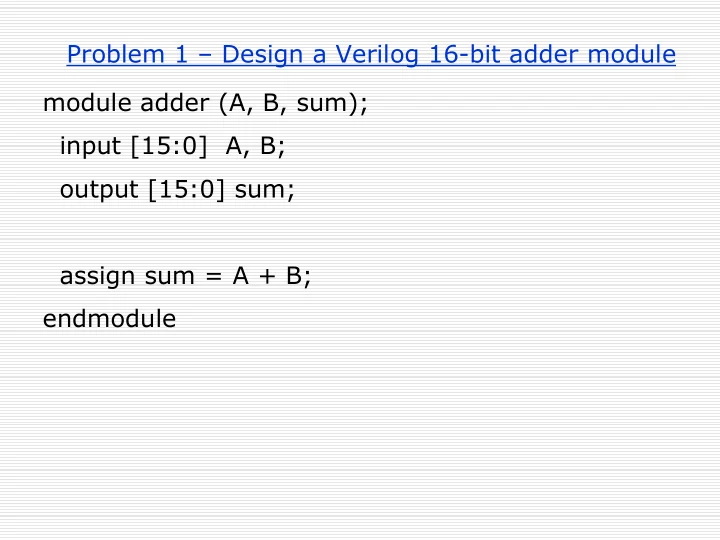
Problem 1 Design a Verilog 16-bit adder module module adder (A, B, sum); input [15:0] A, B; output [15:0] sum; assign sum = A + B; endmodule Problem 1 Design a Verilog 16-bit adder module module adder (A, B, sum); input [15:0] A,
Problem 1 – Design a Verilog 16-bit adder module module adder (A, B, sum); input [15:0] A, B; output [15:0] sum; assign sum = A + B; endmodule
Problem 1 – Design a Verilog 16-bit adder module module adder (A, B, sum); input [15:0] A, B; output [15:0] sum; reg [15:0] sum; always @(A or B) begin sum = A + B; end endmodule
Problem 2 – Design a Verilog 16-bit ALU module alu (A, B, op, result); input [15:0] A, B; input [2:0] op; output [15:0] result; reg [15:0] result; always @(A or B or op) begin case (op) 0: result = A + B; . . . 6: result = B - A; default: result = 16’bX; end endmodule
Problem 2 – Design a Verilog 16-bit ALU module alu (A, B, op, result); input [15:0] A, B; input [2:0] op; output [15:0] result; assign result = (op==0)?(A+B): . . . (op==6)?(B-A): 16’bX; endmodule
Problem 3 – Design a Verilog Register File (write) module rfile (clk, reset AddrA, AddrB, AddrW, A, B, Din, write); reg [15:0] R0, R1, R2, R3; always @(posedge clk) begin case (AddrW) 0: R0 <= Din; 1: R1 <= Din; 2: R2 <= Din; 3: R3 <= Din; endcase endmodule
Problem 3 – Design a Verilog Register File (read) module rfile (clk, reset AddrA, AddrB, AddrW, A, B, Din, write); reg [15:0] R0, R1, R2, R3; always @(AddrA) begin case (AddrA or R0 or R1 or R2 or R3) + The equivalent 0: A = R0; always block for B 1: A = R1; 2: A = R2; 3: A = R3; endcase end endmodule
Restricted FSM Implementation Style � Mealy machine requires two always blocks � register needs posedge CLK block � input to output needs combinational block � Moore machine can be done with one always block � e.g. simple counter � Not a good idea for general FSMs � Can be very confusing (see example) � Moore outputs � Share with state register, use suitable state encoding
Problem 4 – Design a “Steppable” Clock A clock generator: Mode 0 : clk is free-running, 1/2 sysClk frequency Mode 1 : clk is stopped, step causes one pulse on clk Mode clk step sysClk sysClk step clk
Problem 4 – Design a “Steppable” Clock Draw a state diagram – start with Mode 1 (step mode) 0/0 IDLE 1/0 UP 0/0 X/1 DOWN 1/0 sysClk step clk
Problem 4 – Design a “Steppable” Clock Draw a state diagram – start with Mode 1 (step mode) 0 IDLE 1 [0] [1] UP 00 01 0 X State Assignment? [0] Since clk is a Moore output, DOWN share it with a state bit 1 10 sysClk step clk
Problem 4 – Design a “Steppable” Clock Draw a state diagram – start with Mode 1 (step mode) inputs: mode,step 10 IDLE 0X,11 [0] [1] UP 00 01 0X X0 1X Now add the mode input [0] When mode = 0, clk is DOWN free-running X1 10 sysClk step clk
Verilog for “Steppable” Clock (state reg) module stepClk (sysClk, mode, step, clk); input sysClk, mode, step; output clk; parameter IDLE=0, UP=1, DOWN=2; // Use names! reg [1:0] state, nxtState; assign clk = state[0]; // clk output shared with state always @(posedge sysClk) begin state <= nxtState; end 10 IDLE 0X,11 [0] [1] UP 00 01 0X X0 1X [0] DOWN X1 10
Verilog for “Steppable” Clock (functions) module stepClk (sysClk, mode, step, clk); input sysClk, mode, step; output clk; parameter IDLE=0, UP=1, DOWN=2; always @(state or mode or step) begin nxtState = state; // Default (what if we leave out??) case (state) IDLE : if (~mode | step) nxtState = UP; UP : nxtState = DOWN; DOWN : if (~mode) nxtState = UP; else if (~step) nxtState = IDLE; endcase 10 IDLE 0X,11 end [0] [1] UP 00 01 0X X0 1X [0] DOWN X1 10
Verilog for “Steppable” Clock (functions) module stepClk (sysClk, mode, step, clk); input sysClk, mode, step; output clk; parameter IDLE=0, UP=1, DOWN=2; always @(state or mode or step) begin nxtState = state; // Default (does this matter?) case (state) IDLE : if (~mode | step) nxtState = UP; UP : nxtState = DOWN; DOWN : if (~mode) nxtState = UP; else if (~step) nxtState = IDLE; default: nxtState = 2’bX; // Does this matter? endcase end
Problem 5 : Data Switch Two input data streams enter the switch, one item per clock Each contains an address (addrA, addrB) which indicates which output port they want The switch sends each to the desired output port If they contend, then the switch treats them fairly valid outputs indicate if there is a message for that output addrA Avalid 0 Ain Aout addrB Bvalid Bin Bout 1
Problem 5 : Data Switch There is a control and data circuit. Design the data circuit first. Ain 0 Aout 1 1 Bout 0 Bin swap/straight Avalid addrA 0 Ain Aout Bvalid addrB Bin Bout 1
Problem 5 : Data Switch Verilog for data circuit: input [15:0] Ain, Bin; output [15:0] Aout, Bout; reg swap; // Internal Control signal assign Aout = swap ? Bin : Ain; assign Bout = swap ? Ain : Bin; Ain 0 Aout 1 1 Bout 0 Bin swap/straight
Problem 5 : Data Switch Verilog for data circuit: input [15:0] Ain, Bin; // Add reg declaration output [15:0] Aout, Bout; // for always block! reg swap; // Internal Control signal always @(Ain or Bin or swap) begin if (swap) begin Aout = Bin; Bout = Ain; end else begin Aout = Ain; Bout = Bin; end end Ain 0 Aout 1 1 Bout 0 Bin swap/straight
Problem 5 : Data Switch Verilog for data circuit: input [15:0] Ain, Bin; output [15:0] Aout, Bout; reg swap; // Internal Control signal always @(Ain or Bin or swap) begin Aout = Ain; Bout = Bin; // Default if (swap) begin Aout = Bin; Bout = Ain; end end Ain 0 Aout 1 1 Bout 0 Bin swap/straight
Problem 5 : Data Switch AddrA,AddrB/swap Now design the control If we have addrA, addrB and swap, then we can compute Avalid and Bvalid: assign Avalid = (addrA == swap); assign Bvalid = (addrB != swap); 0 addrA Avalid swap addrB Bvalid 1
Problem 5 : Data Switch AddrA,AddrB/swap Now design the control: Mealy! We forward the data this clock cycle 00/0 11/1 APRI BPRI 01/0 01/0 10/1 10/1 00/1 11/0 0 addrA Avalid swap addrB Bvalid 1
Problem 5 : Data Switch Verilog module switch (clk, reset, Ain, addrA, Bin, addrB, Aout, Avalid, Bout, Bvalid); input clk, reset; input [15:0] Ain, Bin; input addrA, AddrB; output [15:0] Aout, Bout; output Avalid, Bvalid; reg swap; // Control signal assign Aout = swap ? Bin : Ain; assign Bout = swap ? Ain : Bin; assign Avalid = (addrA == swap); assign Bvalid = (addrB != swap); parameter APRI=0, BPRI=1; // State names reg state, next_state; always @(posedge clk) begin if (reset) state <= APRI; else state <= next_state; end always @(*) begin next_state = state; swap = 0; case (state) APRI: begin swap = addrA; if (addrA == addrB) nextState = BPRI; end BPRI: begin swap = ~addrB; if (addrA == addrB) nextState = APRI; end endcase APRI 00/0 BPRI end 11/1 endmodule 01/0 01/0 10/1 10/1 00/1 11/0
Recommend
More recommend
Explore More Topics
Stay informed with curated content and fresh updates.
