VERILOG Hardware Description Language CAD for VLSI 1 About - PDF document
VERILOG Hardware Description Language CAD for VLSI 1 About Verilog Along with VHDL, Verilog is among the most widely used HDLs. Main differences: VHDL was designed to support system- level design and specification. Verilog was
VERILOG Hardware Description Language CAD for VLSI 1 About Verilog • Along with VHDL, Verilog is among the most widely used HDLs. • Main differences: – VHDL was designed to support system- level design and specification. – Verilog was designed primarily for digital hardware designers developing FPGAs and ASICs. CAD for VLSI 2 1
Concept of Verilog “Module” • In Verilog, the basic unit of hardware is called a module . – Modules cannot contain definitions of other modules. – A module can, however, be instantiated within another module. – Allows the creation of a hierarchy in a Verilog description. CAD for VLSI 3 Basic Syntax of Module Definition module module_name (list_of_ports); input/output declarations; local net declarations; parallel statements; endmodule CAD for VLSI 4 2
Example 1 :: simple AND gate module simpleand (f, x, y); input x, y; output f; assign f = x & y; endmodule CAD for VLSI 5 Example 2 :: two-level circuit module two_level (a, b, c, d, f); input a, b, c, d; output f; wire t1, t2; assign t1 = a & b; assign t2 = ~ (c | d); assign f = t1 ^ t2; endmodule CAD for VLSI 6 3
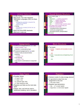
Variable Data Types • A variable belongs to one of two data types: – Net • Must be continuously driven • Used to model connections between continuous assignments & instantiations – Register • Retains the last value assigned to it • Often used to represent storage elements CAD for VLSI 7 Net data type – Different ‘net’ types supported for synthesis: • wire, wor, wand, tri, supply0, supply1 – ‘wire’ and ‘tri’ are equivalent; when there are multiple drivers driving them, the outputs of the drivers are shorted together. – ‘wor’ / ‘wand’ inserts an OR / AND gate at the connection. – ‘supply0’ / ‘supply1’ model power supply connections. CAD for VLSI 8 4
module using_wired_and (A, B, C, D, f); input A, B, C, D; output f; wand f; // net f declared as ‘wand’ assign f = A & B; assign f = C | D; endmodule CAD for VLSI 9 module using_supply_wire (A, B, C, f); input A, B, C; output f; supply0 gnd; supply1 vdd; nand G1 (t1, vdd, A, B); xor G2 (t2, C, gnd); and G3 (f, t1, t2); endmodule CAD for VLSI 10 5
Register data type – Different ‘register’ types supported for synthesis: • reg, integer – The ‘reg’ declaration explicitly specifies the size. reg x, y; // single-bit register variables reg [15:0] bus; // 16-bit bus, bus[15] MSB – For ‘integer’, it takes the default size, usually 32-bits. • Synthesizer tries to determine the size. CAD for VLSI 11 Other differences : – In arithmetic expressions, • An ‘integer’ is treated as a 2’s complement signed integer. • A ‘reg’ is treated as an unsigned quantity. – General rule of thumb • ‘reg’ used to model actual hardware registers such as counters, accumulator, etc. • ‘integer’ used for situations like loop counting. CAD for VLSI 12 6
module simple_counter (clk, rst, count); input clk, rst; output count; reg [31:0] count; always @(posedge clk) begin if (rst) count = 32’b0; else count = count + 1; end endmodule CAD for VLSI 13 • When ‘integer’ is used, the synthesis system often carries out a data flow analysis of the model to determine its actual size. • Example: wire [1:10] A, B; integer C; C = A + B; � The size of C can be determined to be equal to 11 (ten bits plus a carry). CAD for VLSI 14 7
Specifying Constant Values • A value may be specified in either the ‘sized’ or the ‘un-sized’ form. – Syntax for ‘sized’ form: <size>’<base><number> • Examples : 8’b01110011 // 8-bit binary number 12’hA2D // 1010 0010 1101 in binary 12’hCx5 // 1100 xxxx 0101 in binary 25 // signed number, 32 bits 1’b0 // logic 0 1’b1 // logic 1 CAD for VLSI 15 Parameters • A parameter is a constant with a name. • No size is allowed to be specified for a parameter. – The size gets decided from the constant itself (32-bits if nothing is specified). • Examples : parameter HI = 25, LO = 5; parameter up = 2b’00, down = 2b’01, steady = 2b’10; CAD for VLSI 16 8
Logic Values • The common values used in modeling hardware are: 0 :: Logic-0 or FALSE 1 :: Logic-1 or TRUE x :: Unknown (or don’t care) z :: High impedance • Initialization: – All unconnected nets set to ‘z’ – All register variables set to ‘x’ CAD for VLSI 17 • Verilog provides a set of predefined logic gates. – They respond to inputs (0, 1, x, or z) in a logical way. – Example :: AND 0 & 0 � � 0 � � 0 & x � � � 0 � 0 & 1 � � 0 1 & z � � x � � � � 1 & 1 � � 1 � � z & x � � � x � 1 & x � � � � x CAD for VLSI 18 9
Primitive Gates • Primitive logic gates (instantiations): and G (out, in1, in2); nand G (out, in1, in2); or G (out, in1, in2); nor G (out, in1, in2); xor G (out, in1, in2); xnor G (out, in1, in2); not G (out1, in); buf G (out1, in); CAD for VLSI 19 • Primitive Tri-State gates (instantiation) bufif1 G (out, in, ctrl); bufif0 G (out, in, ctrl); notif1 G (out, in, ctrl); notif0 G (out, in, ctrl); CAD for VLSI 20 10
Some Points to Note • For all primitive gates, – The output port must be connected to a net (a wire). – The input ports may be connected to nets or register type variables. – They can have a single output but any number of inputs. – An optional delay may be specified. • Logic synthesis tools ignore time delays. CAD for VLSI 21 `timescale 1 ns / 1ns module exclusive_or (f, a, b); input a, b; output f; wire t1, t2, t3; nand #5 m1 (t1, a, b); and #5 m2 (t2, a, t1); and #5 m3 (t3, t1, b); or #5 m4 (f, t2, t3); endmodule CAD for VLSI 22 11
Hardware Modeling Issues • The values computed can be held in – A ‘wire’ – A ‘flip-flop’ (edge-triggered storage cell) – A ‘latch’ (level-sensitive storage cell) • A variable in Verilog can be of – ‘net data type • Maps to a ‘wire’ during synthesis – ‘register’ data type • Maps either to a ‘wire’ or to a ‘storage cell’ depending on the context under which a value is assigned. CAD for VLSI 23 module reg_maps_to_wire (A, B, C, f1, f2); input A, B, C; output f1, f2; wire A, B, C; reg f1, f2; always @(A or B or C) begin f1 = ~(A & B); f2 = f1 ^ C; The synthesis system end will generate a wire for f1 endmodule CAD for VLSI 24 12
module a_problem_case (A, B, C, f1, f2); input A, B, C; output f1, f2; wire A, B, C; reg f1, f2; always @(A or B or C) begin f2 = f1 ^ f2; f1 = ~(A & B); The synthesis system end will not generate a endmodule storage cell for f1 CAD for VLSI 25 // A latch gets inferred here module simple_latch (data, load, d_out); input data, load; output d_out; always @(load or data) begin if (!load) t = data; d_out = !t; Else part missing; so end latch is inferred. endmodule CAD for VLSI 26 13
Verilog Operators • Arithmetic operators *, /, +, -, % • Logical operators ! � � � logical negation � && � � � logical AND � | | � � logical OR � � • Relational operators >, <, >=, <=, ==, != • Bitwise operators ~, &, |, ^, ~^ CAD for VLSI 27 • Reduction operators (operate on all the bits within a word) &, ~&, |, ~|, ^, ~^ � � � � accepts a single word operand and produces a single bit as output • Shift operators >>, << • Concatenation { } • Replication { n { } } • Conditional <condition> ? <expression1> : <expression2> CAD for VLSI 28 14
// An 8-bit adder description module parallel_adder (sum, cout, in1, in2, cin); input [7:0] in1, in2; input cin; output [7:0] sum; output cout; assign #20 {cout, sum} = in1 + in2 + cin; endmodule CAD for VLSI 29 Some Points • The presence of a ‘z’ or ‘x’ in a reg or wire being used in an arithmetic expression results in the whole expression being unknown (‘x’). • The logical operators (!, &&, | |) all evaluate to a 1-bit result (0, 1 or x). • The relational operators (>, <, <=, >=, ~=, ==) also evaluate to a 1-bit result (0 or 1). • Boolean false is equivalent to 1’b0 Boolean true is equivalent to 1’b1. CAD for VLSI 30 15
Some Valid Statements assign outp = (p == 4’b1111); if (load && (select == 2’b01)) ……. assign a = b >> 1; assign a = b << 3; assign f = {a, b}; assign f = {a, 3’b101, b}; assign f = {x[2], y[0], a}; assign f = { 4{a} }; // replicate four times assign f = {2’b10, 3{2’b01}, x}; CAD for VLSI 31 Description Styles in Verilog Two different styles of description: • 1. Data flow Continuous assignment • 2. Behavioral Procedural assignment • � Blocking � Non-blocking CAD for VLSI 32 16
Recommend
More recommend
Explore More Topics
Stay informed with curated content and fresh updates.
