VELO Upgrade Data Acquisition System Karol Hennessy October 2, 2018 - PowerPoint PPT Presentation
VELO Upgrade Data Acquisition System Karol Hennessy October 2, 2018 University of Liverpool VELO Upgrade Vertex Detector for the LHCb VELO Upgrade Data Acquisition System October 2, 2018 K. Hennessy LHCb 40 MHz readout - full
VELO Upgrade Data Acquisition System Karol Hennessy October 2, 2018 University of Liverpool
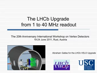
VELO Upgrade • Vertex Detector for the LHCb VELO Upgrade Data Acquisition System — October 2, 2018 — K. Hennessy LHCb 40 MHz readout - full detector readout @ microchannel CO 2 • Requires active cooling - • In vacuum • Very high radiation environment LHC beam interaction region • 52 silicon pixel modules around the upgrade 2 / 37 • LHCb Upgrade has triggerless • 50ħb − 1 integrated luminosity • maximum fluence approx. 8 × 10 15 MeV · n eq / cm 2
VELO Upgrade Data Acquisition System — October 2, 2018 — K. Hennessy 3 / 37
VELO Upgrade CAD VELO Upgrade Data Acquisition System — October 2, 2018 — K. Hennessy 4 / 37
VELO Upgrade Electronics VELO Upgrade Data Acquisition System — October 2, 2018 — K. Hennessy 5 / 37
VELO Upgrade Electronics VELO Upgrade Data Acquisition System — October 2, 2018 — K. Hennessy 6 / 37
VELO Upgrade in Numbers Feature VELO Upgrade Data Acquisition System — October 2, 2018 — K. Hennessy 2.2-2.3 kW Total Power consumption 2+ Tb/s Total data rate 40 MHz ASIC Readout rate 1000 V HV tolerance Max fluence electron collecting Technology 0.12 m 2 Detector Active area 52 # of modules Pixels Sensors 7 / 37 ∼ 41 M pixels 200 µ m thick 8 × 10 15 MeVn eq / cm − 2
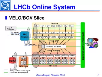
Pathways ECS - Experiment Control System • 4.8 Gb/s • Use of GBLD as electrical line driver (emphasis and amplification functionality) DAQ - Data Acquisition back-end) • 5.12 Gb/s • VeloPix has some internal emphasis Similar electrical transmission lines for ECS and DAQ - expect similar performance. VELO Upgrade Data Acquisition System — October 2, 2018 — K. Hennessy 8 / 37 • Bi-directional with GBTx ASIC • Uni-directional (from VeloPix to
ECS Path VELO Upgrade Data Acquisition System — October 2, 2018 — K. Hennessy 9 / 37
Opto-Power Board • Situated on VELO tank exterior • Vacuum Feedthrough Board interfaces electronics inside VELO tank • Fibres to counting room at surface • Interface for data, control, monitoring signals and powering for VELO modules • DC/DCs for power • Voltage monitoring • Optical transceivers for driving to/from backend • Control via GBT chipset VELO Upgrade Data Acquisition System — October 2, 2018 — K. Hennessy 10 / 37 ( ≈ 300 m)
GBT - ECS interface • All three logical paths can be encapsulated on a single physical interface VELO Upgrade Data Acquisition System — October 2, 2018 — K. Hennessy • The GBTX chip is a radiation tolerant chip for LHC upgrade experiments 11 / 37 • Data Acquisition (DAQ) - (NOT used for VELO) • Trigger and Timing Control (TTC) • GBT Protocol can utilise three logical data paths • Slow Control (SC) - via companion SCA chip GBT GBT Versatile Link Back-End Board Timing & Trigger Timing & Trigger Photo GBTIA DAQ diode GBT- GBTX DAQ FPGA Laser GBT- GBLD diode SCA Slow Control Slow Custom ASICs Versatile Control Transceiver On-Detector Off-Detector
Timing and Fast Control (TFC) • Single Readout Supervisor provides a clock and timing commands to front-end and back-end electronics • BXID Reset, FE Reset, BE Reset, Sync, … • Interfaces with LHC • TFC commands are fixed latency • Data are NOT fixed latency • For VELO, TFC synchronisation commands form “special” GWT packets and sent immediately from front-end • (standard data packets are sent out-of-time) • 10G PON network with optional feedback VELO Upgrade Data Acquisition System — October 2, 2018 — K. Hennessy 12 / 37
DAQ Path VELO Upgrade Data Acquisition System — October 2, 2018 — K. Hennessy 13 / 37
VeloPix ASIC • Front-end ASIC driving the design of the VELO data acquisition system • Designed for high radiation tolerance and low power consumption • Custom output serialiser - Gigabit Wireline Transmitter (GWT) • Slow control via SLVS protocol • 12 VeloPix chips per module • 20 readout links (more links for hotter chips) VELO Upgrade Data Acquisition System — October 2, 2018 — K. Hennessy 14 / 37 • Operates at LHC clock rate ∼ 40MHz
VeloPix ASIC Max data rate VELO Upgrade Data Acquisition System — October 2, 2018 — K. Hennessy • Non-uniform radiation dose tolerant • Radiation hard 400 Mrad, and SEU 2.85 Tb/s Total VELO 20.48 Gb/s 900 Mhits/s/ASIC • Readout is data driven - SuperPixels Peak hit rate readout • Based on the Timepix3 ASIC • Binary readout @ 40 MHz zero-suppression) “hits above threshold” (a.k.a. are only read out when they have 15 / 37 • VeloPix is optimised for high speed • Power consumption < 1.5 W · cm − 2
VeloPix Data readout called SuperPixels • 30% reduction in data size stored in SuperPixel data packet • Custom serializer - Gigabit Wireline Transmitter (GWT) • Low power - 60 mW • 5.12 Gb/s line rate • GWT protocol • scrambled data • parity check, no error recovery VELO Upgrade Data Acquisition System — October 2, 2018 — K. Hennessy 16 / 37 • Pixel data is aggregated into groups of 2 × 4 • Data is sent out-of-time ⇒ timestamp • ⇒ minimise bit error rate
Backend DAQ and Slow Control - PCIe40 • Single control and readout board for VELO Upgrade Data Acquisition System — October 2, 2018 — K. Hennessy (measured). • 48 bi-directional links (or 96 DDR4) ESC4000-G3, 2x Xeon 3 GHz, 8x 8 GB • up to 4 PCIe40 per chassis (ASUS 80W FPGA, 157W card • High power consumption - up to • PCIe Gen3 x16 components • Common hardware, shared firmware • Can be used for TFC, SC, or DAQ or all the entire experiment 17 / 37 • Intel Arria10 FPGA (10AX115S4F45E3SG) uni-directional) @ ∼ 5 Gb/s • Output bandwidth 100 Gb/s
MiniDAQ - All in one solution • MiniDAQ = PCIe40 + server • The MiniDAQ platform allows for controls, DAQ, and soħtware all to run in a standalone system • The server is provided with the PCIe40 installed, necessary programming cables and OM3 fibres • WinCC JCOP soħtware comes pre-installed (a licence is needed) • All necessary drivers and support soħtware is installed • With one server, one can control the front-end hardware and at the same time read out its data. VELO Upgrade Data Acquisition System — October 2, 2018 — K. Hennessy 18 / 37
VELO Firmware
VELO Upgrade Data Acquisition System — October 2, 2018 — K. Hennessy 19 / 37
VELO Firmware VELO Upgrade Data Acquisition System — October 2, 2018 — K. Hennessy 20 / 37
VELO Firmware • VELO SOL40 VELO Upgrade Data Acquisition System — October 2, 2018 — K. Hennessy • Phi Ordering • SuperPixel Isolation flagging (proto-clustering) • Optional components (if FPGA resources allow) • Re-ordering the data in time • Router • SuperPixel packet extraction • TFC Synchronisation functionality • Parity check • Descrambling • GWT word alignment • GWT LLI • Requires custom SLVS component in the SOL40 firmware • GBTx is connected directly to the VeloPix rather than through the SCA 21 / 37 • Primary function of the Velo firmware
BXID Router • Latency limit < 512 clock cycles VELO Upgrade Data Acquisition System — October 2, 2018 — K. Hennessy • Time-ordering SuperPixel data 22 / 37 FPGA resource usage • 9-bit router sorts data 1 bit at a time maximise speed (>160 MHz) and minimise • Extensive simulation required - both to 600000 E ✁ ciency from Simulation : 99.99% * 500000 * no analog pile-up Peak at 64 included (highest hit rate in SP 63) # Packets 400000 300000 9-bit BXID (512 clks) su ✁ cient! 200000 100000 0 0 20 40 60 80 100 120 140 160 180 Latency (clk cycles @ 40 MHz
VeloPix Simulation/Emulation • Emulating VeloPix using LHCb Monte-Carlo data VELO Upgrade Data Acquisition System — October 2, 2018 — K. Hennessy 23 / 37 • Hardware emulation using FPGA (Xilinx VC709) • Soħtware emulation for simulation Average number of SuperPixel Packets v Chip limit for chips with: 4 links number of SuperPixels 14 LHCb VELO Simulation 12 10 8 2 links 6 1 link 4 2 0 100 200 300 400 500 600 chip number
Soħtware and Testing
ECS Soħtware • Soħtware for configuring the electronics and readout • Joint COntrols Project @ CERN (JCOP) VELO Upgrade Data Acquisition System — October 2, 2018 — K. Hennessy 24 / 37
ECS Soħtware • Control system modelled with finite state machine tree • commands propagate down; status propagates up • Integrates with SOL40, TELL40, SODIN • Can integrate with COTS hardware (CAEN, ISEG, Wiener…) • Rapid development • Oracle database backed • Archiving, trending, alarm functionality… VELO Upgrade Data Acquisition System — October 2, 2018 — K. Hennessy 25 / 37
Link Performance VELO Upgrade Data Acquisition System — October 2, 2018 — K. Hennessy 26 / 37
MiniDAQ2 Transceiver testing • Goals • Mitigate the kind of transceiver problems seen with MD1 • Generate working transceiver block for GWT with 240 MHz reference (change from MD1) • Use PRBS signals between VC709 Xilinx board and MD2 • Use independent clocks and recover signals in both directions VELO Upgrade Data Acquisition System — October 2, 2018 — K. Hennessy 27 / 37
Recommend
More recommend
Explore More Topics
Stay informed with curated content and fresh updates.
