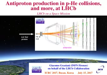
The LHCb Upgrade from 1 to 40 MHz readout The 20th Anniversary - PowerPoint PPT Presentation
The LHCb Upgrade from 1 to 40 MHz readout The 20th Anniversary International Workshop on Vertex Detectors 19-24 June 2011, Rust, Austria Abraham Gallas for the LHCb VELO Upgrade Outline: The LHCb upgrade: scenario & strategy The
The LHCb Upgrade from 1 to 40 MHz readout The 20th Anniversary International Workshop on Vertex Detectors 19-24 June 2011, Rust, Austria Abraham Gallas for the LHCb VELO Upgrade
Outline: • The LHCb upgrade: scenario & strategy • The Vertex detector upgrade: • Environment & plan • Detector module design & layout • Sensor options • ASIC design • Data readout rates • RF foil and material constraints • Cooling • Prototyping results from test beams • Summary 2
The LHCb upgrade • The Plan: • LHCb is currently running with excellent performance at higher luminosity than the nominal: L = 2 10 32 cm – 2 s -1 The experiment will collect ~ 5fb -1 before the 2 nd LHC shutdown circa • 2017 will largely cover the Physics goals of the experiment • During this shutdown we want to upgrade the detector to run at higher luminosity: L = 10 33 cm – 2 s -1 to collect 50 fb -1 (5fb -1 /year) and increased energy √ s = 14 TeV • This does not depend on any (HL)-LHC machine upgrade 3
The LHCb upgrade • Problem : The L0 hadron hardware trigger loses efficiency at higher luminosities: • Because the DAQ event readout rate is limited to 1MHz trigger thresholds (E T ) need to be raised… • Solution : • No hardware trigger, increase the readout rate to 40MHz and implement a fully software-based trigger in the CPU farm Upgraded DAQ Current DAQ LLT Front-end Front-end L0 40MHz L0-buffer Tell40 + 1MHz LLT-buffer Tell1 5-10MHz 1MHz router router 5-10MHz 1MHz CPU-farm CPU-farm Max 3 kHz Max 20 kHz 4 Storage Storage ~ 50 kB ~ 100 kB
Environment: radiation challenge Severe & non-uniform irradiation damage . The sensors edges placed at 7mm from the beam line during “stable beams” . After 50 fb -1 they see a Dose after 50 fb -1 fluence > 4x10 15 1 MeV n eq cm -2 185 MRad or 4.1 10 15 n eq /cm 2 Recent RD50 studies have shown that silicon irradiated at these levels still delivers a signal of ~ 10ke - / MIP 7mm After that dose, we expect currents of ~120 m A/cm 2 @ -15 ° C and V bias = 900 V Danger of thermal runaway at the tip of the sensor from bulk current and heat injected by ROC • Efficient heat removal mandatory to avoid thermal runaway!! • Low noise electronics to cope with reduced signal 5
Environment: data rate challenge Particle occupancy per event (simulation) • Electronics has to digitize, zero suppress and transmit event Particle Hits / Event / cm 2 ~ 5 particles/cm 2 /event at r=7.0 mm data at 40 MHz • By pixel standards the occupancy of the VELO is miniscule, but the data rate is HUGE radius (cm) Curves fitted to A.r -1.9 • 1 chip O(1cm 2 ) has to transmit Luminosity 2.10 32 5.10 32 10.10 32 20.10 32 (cm -2 s -1 ) Current ~13 Gbit s -1 A= 0.98 1.46 2.46 4.80 • Our current granularity, occupancies = ok but FE electronics and DAQ are not 6
VELO Upgrade plan Different systems of the current VELO 1 will be retained: • • CO 2 cooling plant • LV & HV power supply systems • Vacuum vessel and equipment • Motion system • Major new components: • Detector modules based on pixel sensors • New readout ASIC: ´ VELOPIX ´ Replace • Enhance module cooling interface • New design of low material RF foil between beam and detector vacua Multi Gb s -1 readout system • • Main design concerns: • Efficient cooling to avoid thermal runaway • Handle the huge data rate • Reduce material budget • Maintain if not improve the excellent performance 2 : • Proper time resolution ~ 50 fs • IP resolution ~ 13 + 25/pT μm 1,2 See talk by Kazu AKIBA, Silvia Borghi 7
Velo Pixel module • Sensor tiles: 3 readout ASICs on a ~43mm ~15mm single sensor, with a guard ring Sensor tile : ASIC ASIC ASIC ~500 μm sensor • 2 sensor tiles are mounted on opposite sides of a substrate: Cooling Top Sensor 200um channel 60 μ m Kapon+120 μ m Al • Readout & power traces on the substrate ASIC150um Substrate 400um • Substrate choices: ASIC150um Glue 50um Bot Sensor 200um Connector • CVD diamond : excellent mechanical & thermal properties: => low mass • Carbon fibre/TPG or Al/TPG • Material in sensitive region ~ 0.8% X 0 • Prototype work started using Timepix ROCs (@ CNM). 8
Pixel module & detector layout top tiles, bottom tiles • A „station‟ is made of 8 sensor tiles. • active area ~100% (except ~ 1 mm gap small gaps) • Closest pixel is at 7.5 mm BEAM from the beam center The full detector is composed of 26 stations • The modules on either side of the beam are • staggered to create overlap regions This layout has been simulated to be fully • efficient (~98.3%, 4 hit per track) in the LHCb acceptance 15-250x300mrad Varying spacing along the beam axis. Minimal pitch 24 mm 9
Sensor options R&D • Planar Silicon: • Thin sensors seem well suited to the high fluences • R&D focus is on: • Reducing guard ring size. (closer approach to the beam, better impact parameter resolution) • More exotics solutions: trenches, laser scribing & Al 2 O 3 Sidewall passivation (under investigation) • Reducing thickness. (less X 0 , lower bias voltage) • Several wafers with various manufacturers • CNM/USC : 150 μ m p-in-n sensors, 150-200 μ m n-in-p sensor single ASICs and later in the year 3x1 ASICs tiles • Micron/Liverpool: n-in-p (150 and 300 μ m thick) • VTT: slim edge (active) 50,100 μ m edge, different GR, 50-200 μ m thick Irradiation campaign up to 1.4 x 10 16 MeV n eq /cm 2 : • • Planar silicon + Medipix3 check performance in test beam • Different GR structures to be fabricated at the manufacturers d Dicing distances= 250 μ m, 400 μ m, 600 μ m Distance calculated from the active area. One guard ring. CNM G. Pellegrini et al. 10 Marc Christophersenet al.
Sensor options R&D • 3D sensors: • Lower depletion voltage and low power less critical for thermal runaway • Greater signal charge due to faster collection time (less trapping) potentially super radiation hard • Active edge allows closer approach to beam • Double-sided increase yield and improved areas of inefficiency Fluence (10 15 1 MeV n eq cm -2 ) • Many Medipix /Timepix assemblies available • Diamond p-CVD: • No thermal run away problem! • Very radiation hard • Double act: sensor and thermal path 90 S • Financially affordable for the VELO upgrade r ( total surface ~ 1340 cm 2 ) Produced 1.43 x 1.43 cm 2 , 750 m m thick sensor • • Will produce Timepix assemblies for position resolution studies in testbeam 11
Strip-based alternative design Designed new R & F strip sensors, as „backup‟ • solution in case material budget or power of the pixel detector beyond acceptable levels: 30 m m minimum pitch, 20 x 128 strips per sensor • • Goal : keep occupancies < 0.6 % at 10 33 cm -2 s -1 • Signal to Noise ratio after 50 fb -1 : • Keep strip capacitance low • Remove pitch adapter to FE ROC • 40MHz rad-hard ROC to be designed: • Adapted to low capacitance detector • Programmable ZS data transmission • Possible synergy with ST upgrade Pixels Sensitive area less than 500 m m from • edge. First strip at 7.5 mm from beam Strips • Reduce X 0 • Test of prototypes from Hamamatsu this year 12
ASIC development Timepix(now) Timepix2(end 2011) VELOPIX(2012) 256x256 pixels, size (55 m m x 55 m m) gives equal • spatial precision in both directions, removing the need for double sided modules (factor 2 in • Timepix2 is an important material) step towards VELOPIX • IBM 130 nm CMOS process • Similar front end • 3 modes of operation • Counting mode • Fast column bus • Time of Arrival: ToA • Time over threshold: ToT • Data Driven readout • Low occupancy is suited to ToT measurement, with • Simultaneous T ime o ver no loss from 1 μs deadtime T hreshold and T ime o f Changes needed A rrival measurements • Collaborating in the design • Replace shutter based readout/acquisition scheme by continuous, deadtimeless • Aim to have first VELOPIX (ZS) operation by 2012 • Sustained readout of pixels with maximum flux 5 particles /cm 2 /25 ns • Reduced ToT range and resolution • Add bunchtime identification good within 25 ns 13
ASIC development Timepix2/VELOPIX Analog requirements overlap ~100%: Reduce timewalk: <25 ns @ 1ke - threshold • • Faster preamplifier and discriminator of Timepix2 covers and exceeds this requirement • I krum range 5 …40nA • sensitivity 750 … 6000 e - /25ns 20 ke - signal returns to baseline in 660 … 83 ns • • Reduced non-linearity near threshold • Analog power consumption <10 μW /pixel • Higher preamplifier gain (~50mV/ke - ) reduced ENC ( σ ENC ~ 75 e - ), lower detectable charge (<500 e - ) • reduced linear range (30 ke - ) : better suited to Si – tracking • • Threshold spread after tuning < 30e - 14
Recommend
More recommend
Explore More Topics
Stay informed with curated content and fresh updates.
