The Digital Logic Level Wolfgang Schreiner Research Institute for - PowerPoint PPT Presentation
The Digital Logic Level The Digital Logic Level Wolfgang Schreiner Research Institute for Symbolic Computation (RISC-Linz) Johannes Kepler University Wolfgang.Schreiner@risc.uni-linz.ac.at http://www.risc.uni-linz.ac.at/people/schreine
The Digital Logic Level The Digital Logic Level Wolfgang Schreiner Research Institute for Symbolic Computation (RISC-Linz) Johannes Kepler University Wolfgang.Schreiner@risc.uni-linz.ac.at http://www.risc.uni-linz.ac.at/people/schreine Wolfgang Schreiner RISC-Linz
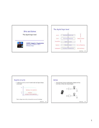
The Digital Logic Level The Digital Logic Level The computer’s real hardware. • Basic elements: gates. • Basic logic: Boolean algebra. • Combinatorial Circuits. • Arithmetic Circuits. • Memory. • CPUs and buses. Boundary between computer science and electrical engineering. Wolfgang Schreiner 1
The Digital Logic Level Gates A gate is a device that computes a function on a two-valued signal. • Fundament: transistor can operate as a binary switch. – Three connections to the outside: collector, base, emitter. – Input voltage V in < critical value: transistor becomes infinite resistance. ∗ Output voltage V out becomes externally regultated voltage V cc (5V). – Input voltage V in > critical value: transistor becomes a wire. ∗ Output voltage V out is pulled to ground (0V). • Interpret voltages as logical values. – “High” voltage ( V cc ) is a logical 1. – “Low” voltage (ground) is a logical 0. Transistor acts like a logical inverter (NOT). Wolfgang Schreiner 2
The Digital Logic Level Basic Gates: Construction +V CC +V CC +V CC V out V 1 Collector V out V out V in V 2 V 1 V 2 Emitter Base (a) (b) (c) NAND and NOR gates can be constructed by wiring two transistors in parallel respectively in series. Wolfgang Schreiner 3
The Digital Logic Level Basic Gates: Logic NOT NAND NOR AND OR A A A A A X X X X X B B B B A X A B X A B X A B X A B X 0 1 0 0 1 0 0 1 0 0 0 0 0 0 1 0 0 1 1 0 1 0 0 1 0 0 1 1 1 0 1 1 0 0 1 0 0 1 0 1 1 1 0 1 1 0 1 1 1 1 1 1 (a) (b) (c) (d) (e) Most computers are based on NAND and NOR gates. Wolfgang Schreiner 4
The Digital Logic Level A B C A B C Boolean Algebra A 1 Algebra of boolean functions. A ABC 4 • Inputs and results are logical values. – Boolean function of n variables has 2 n input combinations. – Representation by truth table with 2 n rows. ABC 5 – 2 2 n Boolean functions with n variables exist. B 2 8 M B A B C M 0 0 0 0 0 0 1 0 6 ABC 0 1 0 0 0 1 1 1 C 1 0 0 0 3 1 0 1 1 C ABC 1 1 0 1 7 1 1 1 1 (a) (b) Wolfgang Schreiner 5
The Digital Logic Level Other Notation Truth tables are too clumsy too handle. • Suffices to specify which combinations of inputs gives output 1. – Let ¯ A denote negation, AB denote conjunction, A + B denote disjunction. – M = ¯ ABC + A ¯ BC + AB ¯ C + ABC . – A function of n variables can be descried by a sum of at most 2 n product terms of n variables. Linear representation of Boolean functions. Wolfgang Schreiner 6
The Digital Logic Level Implementation of Boolean Functions Construct circuit for a given Boolean function. • Systematic process: 1. Write down the truth table for the function. 2. Provide inverters to generate the complement of each input. 3. Draw and AND gate for each term with a 1 in the result column. 4. Wire the AND gates to the appropriate inputs. 5. Feed the output of all AND gates into an OR gate. • Further transformations possible: 1. Replace multi-input gates by two-input gates ( A + B + C + D = ( A + B ) + ( C + D ) ). 2. Replace NOT, AND, OR gates by NAND gates (or by NOR gates). Circuit is not necessarily the simplest one. Wolfgang Schreiner 7
The Digital Logic Level Construction of NOT, AND, OR Any Boolean function can be constructed from NAND or NOR only. A A A A (a) A A AB A + B B B A A AB A + B B B (b) (c) NAND gates and NOR gates are complete. Wolfgang Schreiner 8
The Digital Logic Level Circuit Equivalence Try to reduce the number of gates in a circuit. A AB B A AB + AC A(B + C) B AC C B + C C A B C AB AC AB + AC A B C A B + C A(B + C) 0 0 0 0 0 0 0 0 0 0 0 0 0 0 1 0 0 0 0 0 1 0 1 0 0 1 0 0 0 0 0 1 0 0 1 0 0 1 1 0 0 0 0 1 1 0 1 0 1 0 0 0 0 0 1 0 0 1 0 0 1 0 1 0 1 1 1 0 1 1 1 1 1 1 0 1 0 1 1 1 0 1 1 1 1 1 1 1 1 1 1 1 1 1 1 1 (a) (b) Wolfgang Schreiner 9
The Digital Logic Level Integrated Circuits Gates are manufactured in units called Integrated Circuits (ICs). • Square piece of silicon (5 mm × 5 mm). – Gates are deposited on these “chips”. – Multiple chips are mounted in packages of e.g. 15 mm × 50mm. V CC – Two parallel rows of pins are placed on long edges. 14 13 12 11 10 9 8 Pin 8 • Various integration scales. – SSI (Small Scale Integrated): 1–10. – MSI (Medium Scale Integrated): 10–100. Notch – LSI (Large Scale Integrated): 100–100.000. – VLSI (Very Large Scale Integrated): > 100.100. 1 2 3 4 5 6 7 GND Today: up to 10 million transistors per chip. Wolfgang Schreiner 10
The Digital Logic Level Combinatorial Circuits Wolfgang Schreiner 11
The Digital Logic Level Multiplexers • 2 n data inputs, one data outputs, 1 control input. – Control input selects one of the data inputs. D 0 – Selected input is routed to the output. D 1 • Inverse is demultiplexer. D 2 – 1 data inputs, 2 n outputs, 1 control input. D 3 – Input is routed to the selected output. F D 4 D 5 Fundamental routing operations. D 6 D 7 A A B B C C A B C Wolfgang Schreiner 12
The Digital Logic Level Decoders • n -bit number as input, 2 n output lines. D 0 D 1 – Input selects output line which is set to 1. • Example application: D 2 A A – Memory of eight 1MB chips. D 3 A – 0–1MB, 1-2MB, . . . B B D 4 – Address is presented to memory. B – High-order 3 bits are used to select one chip. D 5 C C C D 6 Fundamental control operations. D 7 Wolfgang Schreiner 13
The Digital Logic Level Arithmetic Circuits Wolfgang Schreiner 14
The Digital Logic Level Adders Exclusive OR gate A B Sum Carry • Half adder. A 0 0 0 0 Sum B – Two inputs, two outputs. 0 1 1 0 1 0 1 0 – Sum of inputs in one output. 1 1 0 1 – Carry in other output. Carry in Carry Carry� Carry� • Full adder. A B Sum in out A Sum 0 0 0 0 0 B – Three inputs, two outputs. 0 0 1 1 0 – Sum of inputs in one output. 0 1 0 1 0 0 1 1 0 1 – Carry but in other output. 1 0 0 1 0 1 0 1 0 1 1 1 0 0 1 Basis of 1 bit ALU. 1 1 1 1 1 Carry out (a) (b) Wolfgang Schreiner 15
The Digital Logic Level Arithmetic Logic Units Logical unit Carry in • 1 bit ALU. AB – Inputs enabled or not (set to 0). INVA A + B A Output ENA – Control input selects operation. B B ENB – AND, OR, NOT, Addition. Sum Basis of n bit ALU. Enable� lines F 0 Full� adder F 1 Decoder Carry out Wolfgang Schreiner 16
The Digital Logic Level Arithmetic Logic Units • 8 bit ALU. – Connection of 1-bit ALU slices. A 7 B 7 A 6 B 6 A 5 B 5 A 4 B 4 A 3 B 3 A 2 B 2 A 1 B 1 A 0 B 0 F 0 F 1 1-bit� 1-bit� 1-bit� 1-bit� 1-bit� 1-bit� 1-bit� 1-bit� INC ALU ALU ALU ALU ALU ALU ALU ALU O 7 O 6 O 5 O 4 O 3 O 2 O 1 O 0 Carry� Carry� in out n -bit ALUs can be constructed from 1-bit slices. Wolfgang Schreiner 17
The Digital Logic Level Memory Wolfgang Schreiner 18
The Digital Logic Level Clocks In digital circuits, timing relations must be controlled. • Clock: circuit that emits sequence of pulses (crystal oscillator). – Precise pulse width; precise interval between pulses (clock cycle time). • Derived clock signals can be constructed by delays. – By combination, clock cycle can be divided in subcycles. C1 C2 Delay (a) (b) A B C (c) Wolfgang Schreiner 19
The Digital Logic Level Latches Circuits that remember “previous” input values. • SR latch. – S input: sets the latch; R input: resets the latch. – If S is 1 and R is 0, Q gets 1. – If R is 1 and S is 0, Q gets 0. – If R and S are 0, Q remains unchanged. – ¯ Q is inverse of Q . 0 0 S S 1 0 Q Q A B NOR 0 1 0 0 1 0 1 0 1 0 0 1 0 1 1 0 Q Q 0 1 R R 0 0 (a) (b) (c) Wolfgang Schreiner 20
The Digital Logic Level Pulse Generators Circuits which generates very short pulses. • A signal a and its negation b are fed into an AND gate. – When signal a is set, negation b is slightly delayed. – For a short period, there is a signal on output d . d ∆ a b b AND c d c c (a) b a Time (b) Wolfgang Schreiner 21
The Digital Logic Level Flip-Flops Circuit which stores a data value at a precise time. • Combination of a pulse generator and a latch. – Inputs of latch are D AND ¯ D (no inconsistency may occur between R and S ). – Inputs are conjoined with output of pulse generator (input is read at well-defined time). D Q Q Current value of D is read and stored a fixed time after clock signal. Wolfgang Schreiner 22
Recommend
More recommend
Explore More Topics
Stay informed with curated content and fresh updates.
