Lecture 02: Digital Logic Review Bei Yu byu@cse.cuhk.edu.hk - PowerPoint PPT Presentation
CENG 3420 Lecture 02: Digital Logic Review Bei Yu byu@cse.cuhk.edu.hk CENG3420 L02 Digital Logic. 1 Spring 2018 Review: Major Components of a Computer CENG3420 L02 Digital Logic. 2 Spring 2018 Review: The Instruction Set Architecture
CENG 3420 Lecture 02: Digital Logic Review Bei Yu byu@cse.cuhk.edu.hk CENG3420 L02 Digital Logic. 1 Spring 2018
Review: Major Components of a Computer CENG3420 L02 Digital Logic. 2 Spring 2018
Review: The Instruction Set Architecture (ISA) software instruction set architecture hardware The interface description separating the software and hardware CENG3420 L02 Digital Logic. 3 Spring 2018
Analog vs. Digital Analog Signal Digital Signal q Vary in a smooth way over q Maintains a constant level time then changes to another constant level (generally q Analog data are operate in one of the two continuous valued states) ● Example: audio, video q Digital data are discrete valued ● Example: computer data CENG3420 L02 Digital Logic. 4 Spring 2018
Number Systems q An ordered set of symbols, called digits, with relations defined for addition, subtraction, multiplication, and division q Radix or base of the number system is the total number of digits allowed in the number system q Commonly used numeral systems CENG3420 L02 Digital Logic. 5 Spring 2018
Conversion from Decimal Integer q Step 1: Divide the decimal number by the radix (number base) q Step 2: Save the remainder (first remainder is the least significant digit) q Repeat steps 1 and 2 until the quotient is zero q Result is in reverse order of remainders CENG3420 L02 Digital Logic. 7 Spring 2018
EX: L02-1 q EX1: Convert 36 8 to binary value q EX2: Convert 36 10 to binary value CENG3420 L02 Digital Logic. 8 Spring 2018
Unsigned Binary Representation Hex Binary Decimal 0x00000000 0…0000 0 0x00000001 0…0001 1 2 31 2 30 2 29 . . . 2 3 2 2 2 1 2 0 bit weight 0x00000002 0…0010 2 31 30 29 . . . 3 2 1 0 bit position 0x00000003 0…0011 3 1 1 1 . . . 1 1 1 1 bit 0x00000004 0…0100 4 0x00000005 0…0101 5 0x00000006 0…0110 6 1 0 0 0 . . . 0 0 0 0 - 1 0x00000007 0…0111 7 0x00000008 0…1000 8 0x00000009 0…1001 9 2 32 - 1 … 2 32 - 4 0xFFFFFFFC 1…1100 2 32 - 3 0xFFFFFFFD 1…1101 2 32 - 2 0xFFFFFFFE 1…1110 2 32 - 1 0xFFFFFFFF 1…1111 CENG3420 L02 Digital Logic. 9 Spring 2018
Signed Binary Representation 2’sc binary decimal -2 3 = 1000 -8 -(2 3 - 1) = 1001 -7 1010 -6 1011 -5 complement all the bits 1100 -4 1101 -3 1011 0101 1110 -2 and add a 1 1111 -1 and add a 1 0000 0 0001 1 1010 0110 0010 2 complement all the bits 0011 3 0100 4 0101 5 0110 6 0111 7 2 3 - 1 = CENG3420 L02 Digital Logic. 10 Spring 2018
EX: L02-2 q For an n-bit signed binary numeral system, what’s the largest positive number and the smallest negative number? CENG3420 L02 Digital Logic. 11 Spring 2018
Digital Signal Representation q Active HIGH ● High voltage means On q Active LOW ● Low voltage means On 5.0 V Logic 0 Logic 1 HIGH (1) 4.0 V False True Off On 3.0 V LOW HIGH 2.0 V No Yes LOW (0) 1.0 V Open Closed switch switch 0.0 V CENG3420 L02 Digital Logic. 12 Spring 2018
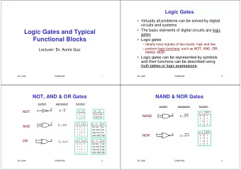
Logic Gates OR AND NOT (Invertor) Invertor schematic view NAND NOR XOR XNOR q What is the schematic view of an AND gate? CENG3420 L02 Digital Logic. 13 Spring 2018
EX: L02-3 q Please draw NOR gate schematic view CENG3420 L02 Digital Logic. 14 Spring 2018
Truth Table q A means for describing how a logic circuit’s output depends on the logic levels present at the circuit’s inputs q The number of input combinations will equal 2 N for an N-input truth table Inputs Output A B Y 0 0 0 A Logic Y 0 1 0 Circuit B 1 0 0 1 1 1 CENG3420 L02 Digital Logic. 15 Spring 2018
EX: L02-4 Determine the true table of a three-input AND gate CENG3420 L02 Digital Logic. 16 Spring 2018
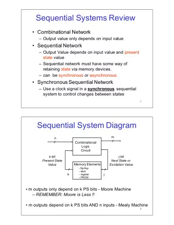
Digital Circuits • Digital circuits generally contain two parts: • Combinational logic • Sequential logic • Combinational circuits consist of logic gates with inputs and outputs • The outputs at any instance of time depend only on the combination of the input values based on logic operations such as AND, OR etc. • Sequential circuits, in addition to inputs and outputs also have storage elements, therefore the output depends on both the current inputs as well as the stored values CENG3420 L02 Digital Logic. 17 Spring 2018
Combinational Circuits Input Output . . Combinational X Z . . Circuits Z = F(X) In combinational circuits, the output at any time is a direct function of the applied external inputs CENG3420 L02 Digital Logic. 18 Spring 2018
Design Procedure of Combinational Circuits Circuit Specification Truth Table How many input/output? Minimization K-maps, Algebraic Manipulation, CAD tools Logic Diagram CENG3420 L02 Digital Logic. 19 Spring 2018
EX: L02-5 q Implement AB+CD using NAND gates only CENG3420 L02 Digital Logic. 20 Spring 2018
Propagation Delay q The delay when the signal arrives at the input of a circuit, and when the output of the circuit changes, is called the propagation delay q A circuit is considered to be fast, if its propagation delay is small (ideally as close to 0 as possible) X Z Y Delay between input (X, Y) and change in output Z CENG3420 L02 Digital Logic. 21 Spring 2018
Timing Diagram q The inputs to a circuit can be changed over time. q The timing diagram shows the values of the input signals to a circuit with the passage of time, in the form of a waveform q It also shows a waveform for the output Propagation X Inputs Delay of the Y Circuit = τ Output Z Timing Diagram for an AND gate Time CENG3420 L02 Digital Logic. 22 Spring 2018
Power Consumption V DD Dynamic Power ≈ C L V DD 2 /2 V o V i C L Ground CENG3420 L02 Digital Logic. 23 Spring 2018
Fanin q Fanin of a gate is the number of inputs to the gate q For a 3-input OR gate, the fanin = 3 q There is a limitation on the fanin for any gate q In CMOS IC technology, higher fanin implies slower gates (higher propagation delays) CENG3420 L02 Digital Logic. 24 Spring 2018
Fanout q Fanout is the number of gates that can be driven by a driver gate q The driven gate is called the load gate q There is a limit to the number of load gates that can be driven by a driver gate Fanout = 3 CENG3420 L02 Digital Logic. 25 Spring 2018
Buffers q Buffers have a single input and a single output, where output = input q Buffers help increase the driving capability of a circuit by increasing the fanout q Drive strength: how much load a gate can drive q Greater drive strength, fanout gates (dis)charged quickly CENG3420 L02 Digital Logic. 26 Spring 2018
How to increase drive strength? q Reduce resistance -> Increase output current ● Increase transistor size with gate ● Parallel a number of transistors BUF_X1 BUF_X4 NAND BUF_X16 CENG3420 L02 Digital Logic. 27 Spring 2018
Decoder n-to-2 n 2 n outputs . n inputs . . Decoder . q Information is represented by binary codes q Decoding - the conversion of an n-bit input code to an m-bit output code with n <= m <= 2 n such that each valid code word produces a unique output code q Circuits that perform decoding are called decoders q A decoder is a minterm generator CENG3420 L02 Digital Logic. 28 Spring 2018
Decoder (Use Cases) q Decode a 3-bit op-codes: q Home automation: Add Sub And op0 3-to-8 Xor op1 Light Decoder Not 2-to-4 op2 A/C C 0 Load Decoder Door C 1 Store Light-A/C Jump Load a Add b Store c . . CENG3420 L02 Digital Logic. 29 Spring 2018
Decoder-Based Circuits S = ∑ (1,2,4,7) C = ∑ (3,5,6,7) X Y Z C S 3 inputs and 8 possible minterms 0 0 0 0 0 3-to-8 decoder can be used for implementing this circuit 0 0 1 0 1 0 1 0 0 1 0 1 1 1 0 1 0 0 0 1 1 0 1 1 0 1 1 0 1 0 1 1 1 1 1 Src: Mano’s book CENG3420 L02 Digital Logic. 30 Spring 2018
Encoder 2 n -to-n 2 n inputs . n outputs . . Encoder . q Encoding - the opposite of decoding - the conversion of an m-bit input code to an n-bit output code such that each valid code word produces a unique output code q Circuits that perform encoding are called encoders q An encoder has 2 n (or fewer) input lines and n output lines which generate the binary code corresponding to the input values q Typically, an encoder converts a code containing exactly one bit that is 1 to a binary code corresponding to the position in which the 1 appears. CENG3420 L02 Digital Logic. 31 Spring 2018
Multiplexers q Directs one of 2 n input to the output q Input to output direction is done based on a set of n select bits � 2 n x 1 2 n inputs one output MUX n select lines CENG3420 L02 Digital Logic. 32 Spring 2018
MUX-based Design (n-1 Select lines) A B C F F(A,B,C)=∑(1,2,6,7) 0 0 0 0 F = C 0 0 1 1 C D 0 C’ D 1 0 1 0 1 F D 2 F = C’ 0 S 1 S 0 0 1 1 0 D 3 1 1 0 0 0 F = 0 A B 1 0 1 0 1 1 0 1 F = 1 1 1 1 1 CENG3420 L02 Digital Logic. 33 Spring 2018
Combinational vs Sequential inputs X outputs Z Combinational Circuits q A combinational circuit: q At any time, outputs depend only on inputs ● Changing inputs changes outputs q History is ignored ! CENG3420 L02 Digital Logic. 34 Spring 2018
Recommend
More recommend
Explore More Topics
Stay informed with curated content and fresh updates.
