Structured Hardware Design Six lectures for CST Part Ia (50 - PDF document
Structured Hardware Design Six lectures for CST Part Ia (50 percent). Easter Term 2004. (C) DJ Greaves. 1 Preface There are a few more slides here than will be used in lectures. At least 10 minutes or so of each lecture will be devoted to
Structured Hardware Design Six lectures for CST Part Ia (50 percent). Easter Term 2004. (C) DJ Greaves. 1
Preface There are a few more slides here than will be used in lectures. At least 10 minutes or so of each lecture will be devoted to example material, including pre- vious exam questions, for which there are no slides in this handout. 2
Books related to the course Suggested books include: W.Ditch. ‘Microelectronic Systems, A practi- cal approach.’ Edward Arnold. The final chap- ters with details of the Z80 and 6502 are not relevant to this course. Floyd. ‘Digital Fundamentals’ Prentice Hall International. T.J. Stoneham. ‘Digital Logic Techniques’ Chapman and Hall. This is a basic book and relates more to the previous course on Digital Electronics. Randy H Katz. ‘Contemporary logic design.’ 3
Flip-Flop Revision Making a transparent latch from an RS latch: s qb D Q db G Q D enable Q D r enable G Putting two together we get the D-type: X Q D Master Slave Y Clock Q D D Q clock A more optimal circuit: X Q Slave D Y Q Clock D Master D Q In this course, we go upwards from the D-type towards systems. 4
A Broadside Register Clock Broadside D Q register N N Clock Q0 D D0 Q1 D1 D Q2 D2 D Q(N-1) D(N-1) D A broadside register of N bits is made out of N D-types with a commoned clock input. It can hold 2 N different values. 5
A Broadside Register - Verilog Clock Broadside D Q register N N Clock Q0 D0 D Q1 D1 D D2 D Q2 Q(N-1) D(N-1) D parameter N = 8; reg [N-1:0] br_q; always @(posedge clk) begin br_q <= data_in; end 6
A broadside two-to-one multiplexor Select N N DT Y DF N MUX2 Select DT0 Y0 DF0 DT1 Y1 DF1 DT(N-1) Y(N-1) DF(N-1) wire [N-1:0] Y, DT, DF; assign Y = (Select) ? DT: DF; 7
A Simple Structure g din D reg1 D reg2 clock We swap the values between a pair of registers if the guard is false, but a broadside multiplexor introduces a new value into the loop when the guard is enabled. reg [7:0] reg1, reg2; always @(posedge clock) begin reg1 <= (g) ? din: reg2; reg2 <= reg1; end 8
A Dual-Port Register File N N Data out A Data in Read Address A Write Address A A N Write Enable Data out B (wen) clock Read Address B A // Verilog for a dual-read ported register file. input [3:0] write_address, read_address_a, read_address_b; reg [7:0] regfile [15:0] always @(posedge clk) begin if (wen) regfile[write_address] <= din; end wire [7:0] data_out_a = regfile[read_address_a]; wire [7:0] data_out_b = regfile[read_address_b]; Ex: Draw out the full circuit at the gate level! 9
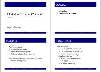
Read Only Memory (ROM) Address In Addr Data Out Data A ROM N PROM Enable Input E or (active low) The ROM contents EPROM are placed inside during manufacture or field programming. The ROM takes A address bits named A0 to A<A-1> and produces data words of N bits wide. For example, if A=5 and D=8 then the ROM contains 2**5 which is 32 locations of 8 bits each. The address lines are called A0, A1, A2, A3, A4 and the data lines D0, D1, ... D7 Access Time Enable Input (active low) Address In High-Z High-Z Data Out Valid data Ouput Turnon Time The ROM’s outputs are high impedance unless the enable input is asserted (low). After the enable is low the output drivers turn on. When the address has been stable sufficiently long, valid data from that address comes out. MASKED PROGRAMMED means contents in- serted at time of manufacture. FLASH PROM uses static electricity on float- ing transistor gates. 10
Read/Write Memory (RAM) Address In Addr A Data In and Out Enable Input Data E RAM (active low) N Read or write R/Wb mode select Read Cycle - Like the ROM Read or write mode select Enable Input (active low) Address In High-Z High-Z Data Bus Valid data Write Cycle - Data stored internally Read or write mode select Enable Input (active low) Address In High-Z Data Bus High-Z Data must be valid here to be stored. Each data bit internally stored in an RS latch. 11
Unlike the edge-triggered flip-flop, the transparent latch passes data through in a transparent way when its enable input is high. When its enable input is low, the output stays at the current value. D Q D Q G G Transparent latch schematic symbol Transparent latch implemented from gates. output enable D D D D D D Data G G G G G G WE* Binary to unary decoder CE* Address Input 12
DRAM MAddr Multiplexed Address In A Data In and Out RAS Data Row Address Strobe (RAS) DRAM N CAS Col Address Strobe (CAS) Read or write R/Wb mode select Read Cycle (write is similar) Read or write mode select Row Address Strobe (RAS) Col Address Strobe (CAS) Multiplexed Address Row Address Col Address High-Z High-Z Data Bus Valid data A DRAM has a multiplexed address bus and the address is presented in two halves, known as row and column addresses. So the capacity is 4**A x D. A 4 Mbit DRAM might have A=10 and D=4. When a processor (or its cache) wishes to read many locations in sequence, only one row address needs be given and multiple col addresses can be given quickly to access data in the same row. This is known as ‘page mode’ access. EDO (extended data out) DRAM is now quite common. This guarantees data to be valid for an exteneded period after CAS, thus helping system timing design at high CAS rates. Refresh Cycle - must happen sufficiently often! Row Address Strobe (RAS) Col Address Strobe (CAS) No data enters or leaves the DRAM during refresh, so it ‘eats memory bandwidth’. Typically 512 cycles of refresh must be done every 8 milliseconds. Modern DRAM has a clock input at 200 MHz and transfers data on both edges. 13
Crystal oscillator clock source 1M 33pF 33pF Ground RC oscillator clock source R Vo Schematic C Symbol Ground Vin 14
Clock multiplication and distribution Outside Inside the the PLL Circuit chip chip 264 MHz VCO External clock Divide 8 input 33 MHz Clock distribution tree Power-on reset Supply R Active low Reset output Vo Vi C Ground 15
Driving a heavy current or high-voltage load High Voltage Supply Load may be Back directly connected EMF or driven through a protection mechanical relay diode Power Control input MOSFT transistor Ground Transistor active area could be 1 square cen- timeter. 16
Debouncer circuit for a two-pole switch +5Volt supply rail Pullup Resistors Output Switch A B Gnd Bounces A B Output 17
ALU and Flags Register Function Code 4 Carry In A-input N Output ALU N B-input N C N Flags register Z V Flags Clock input [7:0] A, B, fc; output [7:0] Y; output C, V, N, Z; always @(A or B or fc) case (fc) 0: { C, Y } = { 1’b0, A }; // A 1: { C, Y } = { 1’b0, B }; // B 2: { C, Y } = A+B; // A+B 3: { C, Y } = A+B; // A+B 4: { C, Y } = A+B+cin; // A+B+Carry in 5: { C, Y } = A-B // and so on ... endcase assign Z = (Y == 0); assign N = y[7]; 18
ALU and Register File Carry In A-input A 8 8 bit Output ALU 8 B-input B Carry Out 8 Function Code D Register file 16 registers Q Din of 8 bits 8 A 4 FUNCTION GEN for F code 4 bit 4 counter Clock source Zero FUNCTION GEN detect for A input An example structure using an ALU and regis- ter file. Ex: Program the ROM function generators to make one large counter out of the whole reg- ister file. 19
Multiplier n n+m n+m-1 if signed m FLASH MULTIPLIER - combinatorial imple- mentation (e.g. a Wallace Tree). BOOTH MULTIPLIER - Does two bits per clock cycle: (* Call this function with c=0 and carry=0 to multiply x by y. *) fun booth(x, y, c, carry) = if(x=0 andalso carry=0) then c else let val x’ = x div 4 val y’ = y * 4 val n = (x mod 4) + carry val (carry’, c’) = case (n) of (0) => (0, c) |(1) => (0, c+y) |(2) => (0, c+2*y) |(3) => (1, c-y) |(4) => (1, c) in booth(x’, y’, c’, carry’) end Ex: Design a controller for an ALU and register file to implement Booth. 20
Logic Symbol Data System Clock N Address Reset Input R A Interrupt Request I Operation Opreq Request Read/Notwrite R/Wb Microprocessor Wait W Internal Structure Block Diagram Addresses Write Clock System Clock Dual Port Register File Function code Load or Store Operation Request ALU Read/notwrite MUX Data Bus Bus Control Execution Unit Control Unit Clock Clock Instruction IR Register OPERAND EA Execution address incrementor Instruction Mux 2 Decoder Reset MUX2 Clock PC Control Wires To Program Address Bus All Other Sections Counter Reset 21
Broadside latch VCC D0 Light emitting diodes Part of data D1 D Q (LEDs) bus D2 D3 Pullup D4 resistors D5 Switches Microprocessor Broadside tri-state GND R/Wbar OPREQ Read from switches A12 A13 Part of address bus Write to A14 leds A15 Example of memory address decode and simple LED and switch interfacing for programmed IO (PIO) to a microprocessor. 22
Recommend
More recommend
Explore More Topics
Stay informed with curated content and fresh updates.
