
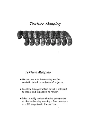
Spiral Content Mapping Combinational Sequential System Level - PowerPoint PPT Presentation
2-1.1 2-1.2 Spiral Content Mapping Combinational Sequential System Level Implementation Spiral Theory Project Design Design Design and Tools Performance Decoders and Structural Verilog 1 metrics (latency muxes
2-1.1 2-1.2 Spiral Content Mapping Combinational Sequential System Level Implementation Spiral Theory Project Design Design Design and Tools • Performance • Decoders and • Structural Verilog 1 metrics (latency muxes • Edge-triggered HDL Spiral 2-1 vs. throughput) • Synthesis with flip-flops • Encoded State • CMOS gate • Boolean Algebra min/maxterms • Registers (with machine design implementation • Canonical • Synthesis with enables) • Fabrication Representations Karnaugh Maps process • Synthesis with 2 • Bistables, • One-hot state • MOS Theory muxes & latches, and Flip- machine design • Capacitance, • Shannon's memory flops • Control and delay and sizing Datapath Components: Theorem • Adder and Counters datapath Memory • • comparator • Memories decomposition constructs design Counters 3 • HW/SW • Power and other partitioning logic families Adders • Bus interfacing • EDA design • Single-cycle CPU process Design Example: Crosswalk Controller 2-1.3 2-1.4 Learning Outcomes • I understand the control inputs to counters • I can design logic to control the inputs of counters to create a desired count sequence • I understand how smaller adder blocks can be combined to form larger ones • I can build larger arithmetic circuits from smaller building blocks DATAPATH COMPONENTS • I understand the timing and control input differences between asynchronous and synchronous memories
2-1.5 2-1.6 Digital System Design • ___________ (CU) and ___________ Unit (DPU) paradigm – Separate logic into datapath elements that operate on data and control elements that generate control signals for datapath elements – Datapath: ___________, _________, comparators, ________, registers (shift, with enables, etc.), memories, FIFO’s – Control Unit: ________________/sequencers clk Control COUNTERS reset … Control … Condition Signals Signals Datapath Data Data Inputs Outputs 2-1.7 2-1.8 Counters Sample 4-bit Counter • Count (Add 1 to Q) at each • 4-bit Up Counter clock edge CE – RST: a synchronous reset P0 Q0 – Up Counter: ____________ P1 Q1 input 4-bit P2 Q2 CNTR – PE and P i inputs: loads Q P3 Q3 – Can also build a down counter as Adder (+) PE with P when PE is active well (____________) TC Q RST – CE: Count Enable Register 1 CLK • Standard counter components • Must be active for the counter to count up include other features – TC (Terminal Count) output CLK RST PE CE Q* – Resets: Reset count to 0 RESET • Active when Q=1111 AND 0,1 counter is enabled – Enables: Will not count at edge if CLK ↑ • TC = __________________ EN=0 – ____________ output ↑ How would you design the • Indicates that on the next ↑ – ______________ Inputs: Can adder block above for a 4-bit edge it will roll over to 0000 counter? ↑ initialize count to a value P (i.e. Q* = P rather than Q+1)
2-1.9 2-1.10 Counters Counter Exercise CLK RST CLK CE RST PE PE P3-P0 1110 CE P[3:0] 0011 1101 1001 1 0000 Q3-Q0 0000 0001 0010 0011 1110 1111 Q[3:0] TC SR=active Q*=Q+1 Enable Q*=Q+1 Q*=Q+1 PE = Q*=Q+1 Q*=Q+1 at clock = off, active, edge, thus thus Q thus Q=0 holds Q=P Mealy TC output: EN•Q3•Q2•Q1•Q0 2-1.11 2-1.12 Counter Design Design a 12-bit Counter (Why TC?) CE • Sketch the design of the 4-bit counter P0 Q0 Q9 Q8 Q7 Q6 Q5 Q4 Q3 Q2 Q1 Q0 P1 Q1 4-bit Q[3:0] P2 Q2 CNTR 0 0 0 0 0 0 0 0 0 0 P3 Q3 presented on the previous slides PE 0 0 0 0 0 0 0 0 0 1 TC RST CLK … 0 0 0 0 0 0 1 1 1 1 0 0 0 0 0 1 0 0 0 0 CE 0 CE P0 Q0 P1 Q1 … 4-bit Q[7:4] P2 Q2 + 0 1 CNTR P3 Q3 0 0 0 0 0 1 1 1 1 1 PE D[3:0] Q[3:0] TC Q[3:0] RST … CLK P[3:0] 1 0 0 1 1 1 1 0 0 0 0 Reg 0 0 1 1 1 1 0 0 0 1 PE CE … P0 Q0 RST CLR Q[11:8] P1 Q1 4-bit P2 Q2 0 0 1 1 1 1 1 1 1 1 CLK CNTR CLK P3 Q3 TC PE 0 1 0 0 0 0 0 0 0 0 TC RST CLK
2-1.13 2-1.14 Counter Example (Using Parallel Inputs) • Design a circuit that counts each clock cycle to produce the pattern 5, 6, 7, 8, 9, 5, 6, 7, 8, 9, 5...9, 5…9,… CE P0 Q0 P1 Q1 ADDERS 4-bit P2 Q2 CNTR P3 Q3 PE TC RST CLK 2-1.15 2-1.16 Adder Intro Adder Intro • So how would we build a circuit • Idea : Build a circuit that performs _____ column of to add two numbers? addition and then use _______________ of those Adder (+) circuits to perform the overall 4-bit addition • Let's try to design a circuit that Q Register 1 can add ANY two 4-bit • Let's start by designing a circuit that adds 2-bits: X numbers, X[3:0] and Y[3:0] and Y that are in the same column of addition – How many inputs? RESET – Can we use K-Maps or sum of CLK minterms, etc? 0110 = X 0110 = X + 0111 = Y + 0111 = Y 1101 1101
2-1.17 2-1.18 Addition – Half Adders Addition – Half Adders C out • We’d like to use one • Addition is done in columns 110 110 adder circuit for each – Inputs are the bit of X, Y 0110 = X 0110 = X column of addition – Outputs are the Sum Bit and Carry-Out (C out ) + 0111 = Y + 0111 = Y • Problem: • Design a Half-Adder (HA) 1101 1101 – No place for __________ circuit that takes in X and Y Sum of last adder circuit and outputs S and C out 0 1 0 1 1 1 • Solution X Y X Y C out S X Y X Y – Redesign adder circuit to Half C out 0 0 0 0 0 Half Half include an ___________ C out Adder 0 C out 1 Adder Adder 0 1 0 1 S ______________ S S 1 0 0 1 1 1 1 1 0 1 0 2-1.19 2-1.20 Addition – Full Adders Addition – Full Adders C out C in • Find the minimal 2-level implementations for Cout and S… • Add a Carry-In input(C in ) 110 • New circuit is called a 0110 = X X Y C in C out S Full Adder (FA) + 0111 = Y • Design the internal 0 0 0 1101 0 0 1 circuitry on the next 0 1 0 slide 0 1 0 1 1 1 0 0 X Y 1 0 1 Full 1 0 1 1 0 C out C in Adder 1 1 1 S 0
2-1.21 2-1.22 Full Adder Logic Addition – Full Adders • Use 1 Full Adder for each column of addition • S = ___________________ – Recall: _____ is defined as true 0110 when ODD number of inputs are true…exactly when the sum bit + 0111 should be 1 • Cout = ____________________ – Carry when sum is 2 or more (i.e. X Y X Y X Y X Y when at least 2 inputs are 1) Full Full Full Full C out C in C out C in C out C in C out C in – Circuit is just checking all Adder Adder Adder Adder combinations of 2 inputs S S S S 2-1.23 2-1.24 Addition – Full Adders Addition – Full Adders • Connect bits of bottom number to Y inputs • Use 1 Full Adder for each column of addition 01100 0110 = X 0110 = X + 0111 = Y + 0111 = Y 1101 0 0 1 1 1 1 0 1 0 0 1 1 1 1 0 1 X Y X Y X Y X Y X Y X Y X Y X Y 0 1 1 0 Full Full Full Full Full Full Full Full 0 C out C in C out C in C out C in C out C in ___ C out C in C out C in C out C in C out C in Adder Adder Adder Adder Adder Adder Adder Adder S S S S S S S S 1 1 0 1
2-1.25 2-1.26 Addition – Full Adders Addition – Full Adders • Use 1 Full Adder for each column of addition • Use 1 Full Adder for each column of addition 01100 01100 0110 = X 0110 = X + 0111 = Y + 0111 = Y 1101 1101 0 0 1 1 1 1 0 1 0 0 1 1 1 1 0 1 X Y X Y X Y X Y X Y X Y X Y X Y 0 1 1 0 0 1 1 0 Full Full Full Full Full Full Full Full C out C in C out C in C out C in C out C in 0 C out C in C out C in C out C in C out C in 0 Adder Adder Adder Adder Adder Adder Adder Adder S S S S S S S S 1 1 0 1 1 1 0 1 2-1.27 2-1.28 Addition – Full Adders Addition – Full Adders • Use 1 Full Adder for each column of addition • Use 1 Full Adder for each column of addition 01100 01100 0110 = X 0110 = X + 0111 = Y + 0111 = Y 1101 1101 0 0 1 1 1 1 0 1 0 0 1 1 1 1 0 1 X Y X Y X Y X Y X Y X Y X Y X Y 0 1 1 0 0 1 1 0 Full Full Full Full Full Full Full Full 0 0 C out C in C out C in C out C in C out C in C out C in C out C in C out C in C out C in Adder Adder Adder Adder Adder Adder Adder Adder S S S S S S S S 1 1 0 1 1 1 0 1
2-1.29 2-1.30 Performing Subtraction w/ Adders Performing Subtraction w/ Adders 0101 • To subtract • To subtract 0101 = X 0101 0101 = X + 1100 - 0011 = Y – Flip bits of Y – Flip bits of Y + 1100 - 0011 = Y 1 0010 1 0010 0010 – Add 1 – Add 1 0010 0 0 1 1 0 1 0 1 1 1 0 0 X Y X Y X Y X Y X Y X Y X Y X Y Full Full Full Full Full Full Full Full C out C in C out C in C out C in C out C in C out C in C out C in C out C in C out C in Adder Adder Adder Adder Adder Adder Adder Adder S S S S S S S S 2-1.31 2-1.32 4-bit Adders Building an 8-bit Adder • 74LS283 chip implements a 4-bit adder • Use (2) 4-bit adders to build an 8-bit adder to add X=X[7:0] and Y= Y[7:0] and produce a sum, S=[7:0] and a carry-out, C8. – Make sure you understand the difference between system labels A 3 A 2 A 1 A 0 = A (actual signal names from the top level design) and device labels + B 3 B 2 B 1 B 0 = B (placeholder names for the signals inside each block). S 4 S 3 S 2 S 1 S 0 = S A 3 B 3 A 2 B 2 A 1 B 1 A 0 B 0 C out C in 74LS283 S 3 S 2 S 1 S 0
Recommend


More recommend
Explore More Topics
Stay informed with curated content and fresh updates.