Spiral 1 / Unit 1 Combinational vs. Sequential Logic Latency vs. - PowerPoint PPT Presentation
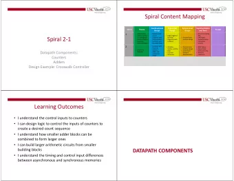
1-1.1 Spiral 1 / Unit 1 Combinational vs. Sequential Logic Latency vs. Throughput (Pipelining) Digital Design Goals Logic Functions 1-1.2 Spiral Content Mapping Combinational Sequential System Level Implementation Spiral Theory Project
1-1.1 Spiral 1 / Unit 1 Combinational vs. Sequential Logic Latency vs. Throughput (Pipelining) Digital Design Goals Logic Functions
1-1.2 Spiral Content Mapping Combinational Sequential System Level Implementation Spiral Theory Project Design Design Design and Tools • • • Performance Decoders and Structural Verilog 1 • metrics (latency muxes Edge-triggered HDL • • • vs. throughput) Synthesis with flip-flops Encoded State CMOS gate • • Boolean Algebra min/maxterms Registers (with machine design implementation • • • Canonical Synthesis with enables) Fabrication Representations Karnaugh Maps process • Synthesis with 2 • • • Bistables, One-hot state MOS Theory muxes & • latches, and Flip- machine design Capacitance, • Shannon's memory • flops Control and delay and sizing • Theorem Adder and • • Counters datapath Memory comparator • Memories decomposition constructs design • • HW/SW Power and other 3 partitioning logic families • • Bus interfacing EDA design • Single-cycle CPU process
1-1.3 Outcomes • I know the difference between combinational and sequential logic and can name examples of each. • I understand latency, throughput, and at least 1 technique to improve throughput • I can identify when I need state vs. a purely combinational function – I can convert a simple word problem to a logic function (TT or canonical form) or state diagram • I can use Karnaugh maps to synthesize combinational functions with several outputs • I understand how a register with an enable functions & is built • I can design a working state machine given a state diagram • I can implement small logic functions with complex CMOS gates
1-1.4 COMBINATIONAL VS. SEQUENTIAL
1-1.5 Combinational vs. Sequential Logic • All logic is categorized into 2 groups – Combinational logic: • Outputs = f(current inputs) – Sequential Logic • Outputs = f(current inputs, previous inputs) • Sequential logic has the notion of “memory” (remembering inputs or events that happened in the past)
1-1.6 Combinational vs. Sequential Current Combinational Outputs Combinational inputs Logic Logic Current inputs Outputs Sequential Sequential Outputs (State) Inputs 1 0 1 feedback as (Next State) inputs Sequential Logic Outputs depend only on current Outputs depend on current inputs outputs and previous inputs (previous inputs summarized via state)
1-1.7 Combinational Example: Staircase Light Switch Light Whether or not the light is S2 on is only dependent on the current position of the switches S1 S1 S2 Light 0 0 0 S1 Logic Light 0 1 1 Circuit 1 0 1 S2 1 1 0
1-1.8 Water Tank Problem • Build a control system for a pump to keep the tank from going empty Pump Pump High Sensor Sensor Low Sensor
1-1.9 Combinational Logic • With combinational logic the outputs only depend on what the inputs are right now A0 S0 A1 4 A2 S1 A3 + 7 ‘283 B0 S2 B1 3 B2 S3 B3 It doesn’t matter what the inputs were previously
1-1.10 Logic Functions • Map input combinations of n-bits to desired m-bit output • Can describe function with a truth table and then find its circuit implementation IN0 IN1 IN2 OUT0 OUT1 0 0 0 0 1 0 0 1 1 1 Logic Inputs Outputs Circuit … 1 1 1 0 0
1-1.11 Logic Example 1 0 A F 1 0 B 0 1 C 1 0 0 D
1-1.12 Sequential Example: Remote Control The channel is a time-dependent function of the first button pressed and the second (we must remember the 3 and then use it with the 2) Time 1 Time 2 Inputting 3 *10 30 channel 32 + 32 2
1-1.13 Flip-Flops • Flip-flops are the building blocks of registers – 1 Flip-flop PER bit of input/output – There are many kinds of flip-flops but the most common is the D- (Data) Flip-flop (a.k.a. D-FF) • D Flip-flop triggers on the clock edge and captures the D-value at that instant and causes Q to remember it until the next edge – Positive Edge: instant the clock transition from low to high (0 to 1) Positive-Edge Triggered D-FF Clock pulse d(t) q(t) D Q d(t) D-FF Clock Signal q(t) CLK
1-1.14 Registers • Registers are the most common sequential device Data Input • (could be Registers sample the data input ( D ) on the D many bits) Data Output edge of a clock pulse ( CP ) and stores that Q (could be value at the output ( Q ) Clock pulse many bits) CP • Analogy: Taking a picture with your digital camera…when you press a button (clock Block Diagram of a Register pulse) the camera samples the scene (input) and remembers/saves it as a snapshot (output) until the next trigger t = 0 ns t = 1 ns t = 5 ns t = 7 ns t = 10 ns Clock pulse Some input value changing over time The clock pulse …causes q(t) to (positive edge) d(t) d(1) d(2) d(3) d(4) d(5) d(6) d(7) d(8) d(9) d(10) d(11) d(12) sample and hold here… the current d(t) q(t) unk d(1) d(5) d(7) d(10) value
1-1.15 Registers and Flip-flops 4-bit Register • A register is simply a group D0 Q0 D Q of D flip-flops that all D-FF trigger on a single clock pulse Q1 D1 D Q D-FF D Q Q2 CLK Q t+1 D2 0 Q t Steady level of 0 D-FF or 1 1 Q t ↑ D t Positive Edge D Q Q3 D3 D-FF CP
1-1.16 Pulses and Clocks • Registers need an edge to trigger Clock Pulses • We can generate pulses at specific times (creating an irregular pattern) when we know the data we want has arrived • Other registers in our hardware should trigger at Clock Signal a regular interval 1 (5V) • For that we use a clock signal… 0 (0V) 1 cycle – Alternating high/low voltage pulse train Op. 1 Op. 2 Op. 3 – Controls the ordering and timing of operations 2.8 GHz = 2.8*10 9 cycles per second performed in the processor = 0.357 ns/cycle – 1 cycle is usually measured from rising/positive edge to rising/positive edge • Processor Clock frequency (F) = # of cycles per second • Clock Period (T) = 1 / Freq.
1-1.17 Summary • Combinational logic – Perform a specific function (mapping of 2 n input combinations to desired output combinations) – No internal state or feedback • Given a set of inputs, we will always get the same output after some time (propagation) delay • Sequential logic (“Storage” devices) – Registers made up of flip-flops/latches are the fundamental building blocks • Controlled by a “clock” signal • Sample data on a “clock” edge and remember that value until the next edge
1-1.18 Combinational vs. Sequential • Sequential logic (i.e. registers) is used to store values ("storage devices") – A register in HW is analogous to a variable in SW (a variable or register stores a value until needed at a later time) • Combinational logic is used to process bits (i.e. perform operations on values – Combinational logic in HW is analogous to operations (+,-,*,&,|,^,<,>) in SW
1-1.19 THROUGHPUT & LATENCY
1-1.20 Performance Depends on View Point?! • What's faster: – A 747 Jumbo Airliner – An F-22 fighter jet • If you are an individual interested in getting from point A to point B, then the F-22 – This is known as latency [units of time] – Time from the start of an operation until it completes • If you are trying to evacuate a large number of people, the 747 looks much better – This is known as throughput [jobs/time]
1-1.21 Throughput vs. Latency • If Latency is the Time it takes to perform 1 Job to complete and Throughput = Jobs / Time … • …Is Throughput = 1 / Latency? • No! – Latency is from the perspective of a single job – Throughput is from the perspective of many jobs – Parallelism is the great friend of throughput! • We will see many times in this course some strategies for improving throughput and sometimes latency
1-1.22 Clocking Methodologies • Typical designs use both combinational and sequential logic – Sequential logic: saves and synchronize data – Combinational logic: performs some operation on the data • Can use feed-forward or feed-back methodology • Clock cycle must be set for the longest path between registers Inputs Sequential Logic Sequential Logic Register Combo Inputs Combo Combo Logic Logic Logic 10 ns 12 ns F = 1/T = 1/___ Combinational Sequential Logic Logic Manipulates Synchronizes & CLK (Processes) Data Save Data CLK Feed-forward Style Feed-back Style
1-1.23 Example for(i=0; i < 100; i++) C[i] = (A[i] + B[i]) / 4; Memory A: i A[i] Cntr B: B[i] C: 10 ns per input set = 1000 ns total
1-1.24 Pipelining Example for(i=0; i < 100; i++) C[i] = (A[i] + B[i]) / 4; Stage 1 Stage 2 Pipelining refers to insertion of registers to Stage 1 Stage 2 split combinational logic Clock 0 A[0] + B[0] into smaller stages that can be overlapped in Clock 1 A[1] + B[1] (A[0] + B[0]) / 4 time (i.e. create an assembly line) Clock 2 A[2] + B[2] (A[1] + B[1]) / 4
Recommend
More recommend
Explore More Topics
Stay informed with curated content and fresh updates.

