Low-Cost 3D Chip Stacking with ThruChip Wireless Connections - PowerPoint PPT Presentation
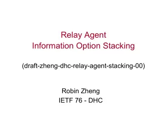
Low-Cost 3D Chip Stacking with ThruChip Wireless Connections Dave.Ditzel@ThruChip.com Tadahiro.Kuroda@ThruChip.com ThruChip Communications October 24, 2014 Stanford EE Computer Systems Colloquium Credit to Professor Tadahiro Kuroda of Keio
Low-Cost 3D Chip Stacking with ThruChip Wireless Connections Dave.Ditzel@ThruChip.com Tadahiro.Kuroda@ThruChip.com ThruChip Communications October 24, 2014 Stanford EE Computer Systems Colloquium
Credit to Professor Tadahiro Kuroda of Keio University Prof Kuroda leads one of the world’s top circuit labs at Keio University. Tadahiro.Kuroda@ThruChip.com Most of the ideas in this talk are from more than a decade of work investigating near-field inductive coupling for 3D stacking by professor Tadahiro Kuroda of Keio University and his students. Kuroda founded ThruChip in 2008, and as ThruChip’s CTO, is helping companies develop lower cost 3D chip stacking. ThruChip provides design information and licensing of professor Kuroda’s inventions. October 24, 2014 ThruChip Wireless 3D Stacking 2
Wireless 3D stacking Current 3D stacking methods have challenges Main challenge is the high cost of Thru Silicon Vias Wireless is a better approach for stacking Lower cost, lower power, higher bandwidth Less costly if we can avoid having to add vertical wires Cost reduction possible, instead of increase, with: Advances in wafer thinning Wireless data communication between stacked die Lower-cost power distribution from front to back of die October 24, 2014 ThruChip Wireless 3D Stacking 3
Challenges with current 3D stacking October 24, 2014 ThruChip Wireless 3D Stacking 4
3D Stacking with Wire Bonds Staircase stacking constrains wire bond access to one side of each die. spacer Pros: Cons: Low Cost High wire bond inductance Good yield Higher power IO Allows ~50 m thin die Bandwidth limited to a few GHz Existing infrastructure Staircase stacking constraints Limited number of bond wires Underside clearance limits die thinness October 24, 2014 ThruChip Wireless 3D Stacking 5
Wire bonding: Pretty example Akita Elpida wire bond example of 20 stacked die(40u pitch) October 24, 2014 ThruChip Wireless 3D Stacking 6
Wire bonding: Not so pretty October 24, 2014 ThruChip Wireless 3D Stacking 7
3D Stacking with Thru Silicon Vias (TSV) Cons: Pros: High Cost (1.4x - 2x) over bare die ~10x lower power IO Requires new CMOS process Thousands of IO possible Yield reductions from bumps Area impact from TSV & KOZ Effects on nearby transistors October 24, 2014 ThruChip Wireless 3D Stacking 8
Proposal for lower cost 3D stacking Separate Data Communication from Power Distribution Data Communication: Use wireless near-field inductive coupling Uses simple CMOS digital circuits: No new semiconductor process expense Provides best in class inter-die power and bandwidth May reduce chip cost if IO area can be reduced Well understood technology validated with dozens of test chips Becomes more compelling as die get thinner Power Distribution: Many options available when wireless used for data Wire bond – Low cost, in high volume production TAB – Low cost, in high volume production RDL/FOWLP – Medium cost, production ready TSV – High cost, early production Recommend Highly Doped Silicon Vias – New lowest cost proposal, discussed later October 24, 2014 ThruChip Wireless 3D Stacking 9
NAND goal is to go From this To this ~1000 m spacer ~80 m Example NAND FLASH NAND FLASH # stacked die 16 16 Die pitch 50 m 5 m Total height ~1000 m ~80 m Die area 1x ~0.9x Data communication wire bond wireless Power delivery wire bond wireless (no metal) IO energy/bit 1x < 1/400x October 24, 2014 ThruChip Wireless 3D Stacking 10
DRAM goal is to go From this To this DRAM die DRAM die ~275 m DRAM die DRAM die ~40 m Base logic die Example DRAM with TSV DRAM # stacked die 5 5 Die pitch 55 m 8 m Total height ~275 m ~40 m Die area 1x 0.87x Data communication TSV wireless Power delivery TSV wireless (no metal vias) IO energy/bit 1x < 1/10x October 24, 2014 ThruChip Wireless 3D Stacking 11
Relevant advances in wafer thinning October 24, 2014 ThruChip Wireless 3D Stacking 12
Ultra-Thin 4 m wafer breakthrough Wafer thinning has been stuck at ~40 m due to “ Gettering problem” Barrier was due in part to loss of the “ gettering effect” at smaller dimensions when performing back grinding, causing impurities affecting device performance (particularly leakage) and yield. DISCO Corporation solution can now thin to a few microns DISCO introduced a “ Gettering Dry Polish” wheel which forms gettering sites while grinding, allowing thinning of wafer silicon to a few microns without device damage. [35] Example: DRAM silicon thinned to 4 microns See “Ultra Thinning down to 4 m m using 300-mm Wafer proven by 40-nm Node 2 Gb DRAM for 3D Multi- stack WOW Applications.”[36] They concluded “No degradation in terms of retention characteristics and distribution employing 2 Gb DRAM wafer was found after ultra- thinning.” 2Gb DRAM thinned to 4 microns Ultra-thin wafers can be handled (from DISCO website) [Reference 36] October 24, 2014 ThruChip Wireless 3D Stacking 13
Wireless 3D data October 24, 2014 ThruChip Wireless 3D Stacking 14
Wireless Near-Field Inductive Coupling Chip designers often spend a lot of time making sure they do not have too much coupling between adjacent wires. Idea: Turn that coupling into an advantage. Use Inductive Coupling for 3D wireless data communication Inductive coils made with a few turns in standard metal layers Coil diameter is about 3x the communication distance Coils communicate vertically to adjacent chips by magnetic field Receive and transmit coils can be placed concentrically on each die to form a transceiver Multiple coils used to increased bandwidth Bandwidth improves with Moore’s law improvement in devices October 24, 2014 ThruChip Wireless 3D Stacking 15
Communication is via magnetic field Receiver Coil dI T V R =k L T L R dt Can easily induce a 200 mV signal in receiver coil. Magnetic field can pass through silicon, including over active circuitry. October 24, 2014 ThruChip Wireless 3D Stacking 16
ThruChip Interface (TCI) Simple transmitter and receiver circuits (basic form shown) Standard digital CMOS: Scales with Moore’s Law Bandwidth: >40 Gigabits/second/coil with modern digital CMOS Delay: About 7 equivalent logic gates (NAND2 FO4) Energy: About 80 equivalent gates Txdata TCI Transmitter Txdata Txdata I T Chip 1 Transmitter Coil Receiver Coil Chip n V R Rxdata TCI Receiver Rxdata Rxdata Time October 24, 2014 ThruChip Wireless 3D Stacking 17
TCI coil example 4 turns xmitter 4 turns receiver 200 m 3 chips with staircase stacking TCI Wireless Transceiver October 24, 2014 ThruChip Wireless 3D Stacking 18
TCI bandwidth vs communication distance 75 5-die stacking D=100 m Coil diameter D=3 x Z D =100 m 70 65 Usable Coil Bandwidth [Gb/s] Usable BW of 66 Gbps Usable circuit bandwidth depends on device Z =32 m 60 55 9 die stacking 50 D =200 m 45 40 35 D=200 m Z =64 m 30 Usable BW of 28 Gbps 25 20 15 D=300 m D=400 m 10 D=500 m 5 32 64 100 150 Communication Distance, Z [ m m] Assumes 8 m die pitch October 24, 2014 ThruChip Wireless 3D Stacking 19
TCI scales with digital CMOS =Measured silicon data =Simulated data Data from references [16,25,28] 100 10000 10 Data Rate, Frequency [Gb/s] 1.5x Energy Dissipation [pJ/b] 1000 1 Delay [ps] 0.1 10 100 80x 7x 10 0.01 1 1 0.001 180 90 65 45 32 180 90 65 45 32 180 90 65 45 32 Process [nm CMOS] Process [nm CMOS] Process [nm CMOS] High BW: Data rate is equivalent to 1.5x of 5-stage ring oscillator Fast: Delay is equivalent to 7x of 2NAND FO4 Low Power: Energy is equivalent to 80x of 2NAND FO4 Small: Circuit layout area is equivalent to 36x 2NAND October 24, 2014 ThruChip Wireless 3D Stacking 20
Energy per Bit becomes very compelling Pin-to-Pin data transfer Node TCI 2 Coils TSV Wire bond 32nm 0.40 pJ/b 0.35 pJ/b 3.45 pJ/b 22nm 0.20 pJ/b 0.30 pJ/b 3.35 pJ/b 16nm 0.10 pJ/b 0.28 pJ/b 3.30 pJ/b 11nm 0.05 pJ/b 0.26 pJ/b 3.27 pJ/b TCI energy will be >65x lower than wire bond, >5x lower than TSV by 11nm. Bus data transfer (8 memory chips + 1 SoC) Node TCI 9 coils TSV Wire bond 32nm 0.40 pJ/b 2.45 pJ/b 24.15 pJ/b 22nm 0.20 pJ/b 2.10 pJ/b 23.45 pJ/b 16nm 0.10 pJ/b 1.96 pJ/b 23.10 pJ/b 11nm 0.05 pJ/b 1.82 pJ/b 22.89 pJ/b TCI energy will be >450x lower than wire bond, >36x lower than TSV by 11nm. October 24, 2014 ThruChip Wireless 3D Stacking 21
Recommend
More recommend
Explore More Topics
Stay informed with curated content and fresh updates.
