SiC and nd diamond amond as s radiat diation ion hard rd - PowerPoint PPT Presentation
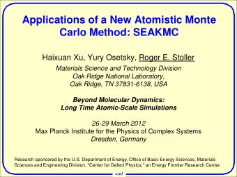
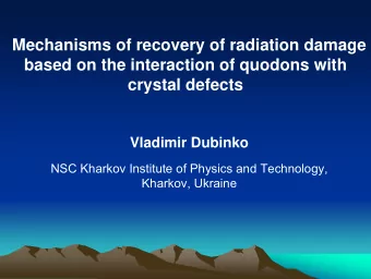
SiC and nd diamond amond as s radiat diation ion hard rd semicondu se conductor or det etec ectors ors Annika Lohstroh Department of Physics, University of Surrey, SEPnet, UK Email: A.Lohstroh@surrey.ac.uk Ackn knowl owledgements
SiC and nd diamond amond as s radiat diation ion hard rd semicondu se conductor or det etec ectors ors Annika Lohstroh Department of Physics, University of Surrey, SEPnet, UK Email: A.Lohstroh@surrey.ac.uk Ackn knowl owledgements edgements Surrey University: CEA (P. Bergonzo, N. Tranchant, C. Deschamps) ESRF (J. Morse) P.J. Sellin I. Gomez Morilla P. Edwards (Strathclyde) S. Gkoumas G. Grime A.W. Davies Element Six Ltd, C. Jeynes P. Veeramani A. Cansell Diamond Detectors Limited M. Hodgson M. Browton EPSRC/STFC/PPARC P. Bryant A.Simon British Council F. Schirru IAEA (CRP: F11016-CR-2) Yusuf Abubakar AWE Page 1
Depar artm tment nt of Phys ysics ics ~ 3 ~ 30 ac acad ademi mics cs Part of he Faculty of Engineering and Physical Sciences (FEPS) • Soft condensed matter (SCM) • Astrophysics • Photonics & Semiconductor devices - Advanced Technology institute (ATI) - in collaboration with electronic engineering • Centre for nuclear and radiation physics (CNRP) Experimental & Theoretical Nuclear Physics Medical and Radiation Physics Medical Physics & Imaging Radiation Detector development 2 academics and approx. 12 research students Page 2
Tal alk k outl tline ine • Basic semiconductor detector operation • Advantages of wide band gap semiconductors – Low Z Radiation hard materials SiC/D • (General) Effects of Radiation damage on semiconductor detector operation • Quantifying “radiation hardness” • Identifying created defects • Conclusion – Future work Page 3
Signa Si nal l forma mation tion V bias E V Bias d Induced current R B _ + _ + Time _ + Signal charge duration sensitive pre- amplifier The current signal is induced by the movement of the created charge carriers: the current is proportional to • the number of carriers lifetime τ > transit time T R • the charge carrier velocity mobility μ , electric field strength Page 4
Signa Si nal l forma mation tion V bias E V Bias d Induced current R B _ + _ + Time _ + Signal charge duration sensitive pre- amplifier Induced charge Signal Time amplitude Page 5
Wid ide e ban and gap ap se semi micon conductor ductor ma mate terials ials for room m te temp mperatur erature e rad adia iation tion dete tector ctor ap applica lication tion Application areas • High energy and nuclear physics • Neutron detection & monitoring in nuclear industry • High energy X- and γ -ray detection for medical http://www.ptw.de/diamond_detector0.html and security applications • Photon science/Synchrotron instrumentation • Medical dosimetry • High fluence backgrounds and harsh environments • .... Commercially available PTW chambers based on natural diamonds Page 6 Page 6
Two ma main in groups ps of ma mate teria ials ls st studied ied High Z material for X/ Radiation hardness/ Tissue “equivalent” spectroscopy and imaging Neutron detection, TOF Birefringence pattern Cd x Zn 1-x Te diamond 3 mm HgI 2 & TlBr http://www.contech.com/Mer 3 mm curic_Iodide_Detectors.htm CdTe CdZnTe Diamond SiC HgI 2 TlBr polymers Page 7
Dia iamo mond nd & Si SiC for se sens nsor r ap applica lication tions Large heat conductance Low Z (low absorption) Tissue equivalence* Wide band gap (solar blind) Fast charge transport * Tissue equivalence* (Radiation) hardness UV sensor Neutron detection (X-ray) Dosimetry Beam monitor (s)LHC * stronger advantage in diamond compared to SiC Page 8
Att ttractive active prope perti rties s for dete tector ctor ap applicat lication ions s (I (II) 80 μ m thick pc CVD diamond Large band gap detector with Al contact “solar blind” (UV detection) (low intrinsic leakage currents) high temperature operation Large heat conductance (5 x copper) Resiliance Chemically inert 1 μ s bunches of 10 9 of 208 Pb 67+ Radiation hardness ions (400 MeV/u =83.2 GeV). => Stable signal (in the order of Ampere) J. Bol et al., phys. stat. sol. (a) 204, 9, pp. 2997-3003 (2007) Page 9
Chal allen lenges ges in in th the ma mate terial ial sy synt nthesis esis Diamond is meta-stable: Several polytypes of SiC exist • High Temperature/High Pressure • Physical Vapour Transport (bulk – single crystal) (HP/HT) limited volume, purity • Chemical vapour deposition (CVD) • Chemical vapour deposition • Heteroepitaxy (typically polycrystalline (CVD) – large area possible) Diamond on Iridium might be able to provide sufficiently thick, Common ommon defects cts homogenous large areas in the Impur puritie ities, s, Vac acancie ncies, s, future Interstit rstitia ials ls • Homoepitaxy (typically < 1 cm 2 area ) Dislocations locations Columnar growth Grain in bound oundar aries ies increasing grain size Stac acking king faults ults towards the top 1 to 10 Poly lyty type pe inclusi lusions ons μ m h -1 Substrate Page 10
50 m) Si SiC – th thick ick (350 m) “bulk” material Bryant et al, IEEE TNS 60(2), pp. 1432 – 1435, 2013 Page 11
Non-un unif ifor orm m respon sponse se in in poly lycrysta crystall llline line ma mate teria ial ) Polycrystalline Single crystalline Columnar growth Signal Amplitude Silver paint increasing grain size Contact edge towards the top Substrate 270 μm 2 296 K 500 μ m Page 12
Ele lectro tronic nic grad ade e si sing ngle le crys ystal tal detect tector or performance ormance Energy resolution similar Time resolution, time of flight: to Silicon 28 ps See Figure 8 and 9 in M. Pomorski et al. phys. stat. sol. (a) 203 (12), pp. 3152-3160 (2006) DOI: 10.1002/pssa.200671127 See Figure 22 in M.Ciobanu, IEEE TNS 58 (4), pp. 2073-2083 (2011) DOI:10.1109/TNS.2011.2160282 Page 13
Towar ards ds la large e ar area a si sing ngle le crys ysta tals ls Images from E. Berdermanet al, 3rd Carat Workshop at GSI, Dec 2011 Heteroepitaxial growth on Iridium – large area substrates possible Main European player: M. Schreck et al in For illustrations see: Augsburg/Germany http://www- carat.gsi.de/CARAT03/CARAT03Talks/B erdermann_CARAT03.pdf Slide 4 and 14 Continuously improvement in thickness, quality and area with time Page 14
Towar ards ds mo more rad adia iation tion har ardness ness Images from B. Caylar et al, 1 st Adamas Workshop at GSI, Dec 2012 For illustrations used see: http://www-adamas.gsi.de/ADAMAS01/talks/caylar.pdf Slide 5 and 19 Several groups have demonstrated working devices: Full CCE reached at very low applied bias (operate detectors with a 9V battery is possible) Page 15
Si SiC – excellent ellent Sc Schottky ttky dio iode des s for Sp Spectros troscopy copy hav ave be been n demo monstrated nstrated Figure 2 in Ruddy et al, Nucl. Instr. Meth. B 263 (2007) 163-168 doi:10.1016/j.nimb.2007.04.077 Page 16
Hig igh h Temp mperat erature re sp spectroscopy troscopy in in epit itaxial axial Si SiC Sc Schottky ttky dio iodes des deve velo loped ed by R y RD50 50) Figure 1 inC. Manfredotti et al., Nucl. Instrum. Meth. A 552 (2005) 131 – 137 doi:10.1016/j.nima.2005.06.018 Alpha emission energy spectrum broad with average energy at 5 MeV (Due to encapsulation of source to be safe to use at elevated Temperature) Page 17
Hig igh h Temp mperat erature re sp spectroscopy troscopy in in Si SiC Page 18
Hig igh h Temp mperat erature re sp spectroscopy troscopy in in Si SiC Stability tests under fast neutron and gamma irradition at room temperature show of epitaxial and bulk SiC samples also show good stability at 4.5 to 18.5 mSv/hour (AmBe Source, Co-60) Page 19
Creat ation ion of defects cts due to to ir irradi adiation ation E K =60 keV 4 fold Energy transfer to the lattice atoms moves them from a substitutional to an interstitial site: Creation of [ V – C i ] (Frenkel pair) Dissociation and diffusion then can lead to many more defect International Journal of Modern Physics C 9, p1x Complexes…… 1998, D. Saada, J. Adler, and R. Kalish K. Schmetzer, The Journal of Annealing can change the defect Gemmology / 2010 / Volume 32 / types and concentrations further No. 1 – 4 Page 20
Effect t of dam amag age e on el n electrica trical l proper perti ties … changes the type/concentration of defects present in the material and hence introduces/removes energy levels in the band gap E C - - • “Close” to E C / E V : - Dopants • Near “mid gap”: Recombination centres E V Page 21
Effect t of dam amag age e on el n electrica trical l proper perti ties … changes the type/concentration of defects present in the material and hence introduces/removes energy levels in the band gap Leakage current: : In an “ideal” intrinsic semiconductor, free E C - - charge carrier density is given by N c , density of - E states in the G n N exp C conduction band 2 k T B ~ 10 19 cm -3 Large E G gives lower dark currents, but experimentally “intrinsic” leakage E V current dominated by free carriers from defect states in the band gap Page 22
Recommend
More recommend
Explore More Topics
Stay informed with curated content and fresh updates.
