Hiroshima Conference HSTD 11 Okinawa, Dec 10 15, 2017 Pixel - PowerPoint PPT Presentation
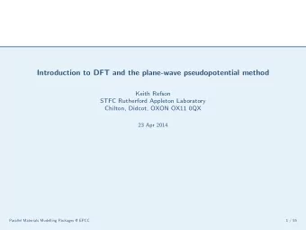
Hiroshima Conference HSTD 11 Okinawa, Dec 10 15, 2017 Pixel Detector Overview Pixel Detectors ... where do we stand ? in my very subjective opinion ... w/ apologies Norbert Wermes University of Bonn 1 N. Wermes, HSTD11, OIST 12/2017
Hiroshima Conference HSTD 11 Okinawa, Dec 10 – 15, 2017 Pixel Detector Overview Pixel Detectors ... where do we stand ? in my very subjective opinion ... w/ apologies Norbert Wermes University of Bonn 1 N. Wermes, HSTD11, OIST 12/2017
~1997 LHC ATLAS/CMS HEP tracking HI Hybrid pixel detectors biomedical AGIPD Imaging MEDIPIX photon science HI, B-FAC ALICE ITS ATLAS CMOS Monolithic pixel detectors HEP tracking LHC 2017 Imaging DSOI pixels 2 N. Wermes, HSTD11, OIST 12/2017
Some early prejudices ... e.g. about HL-LHC radiation levels - Tough for planar sensors ... !? There is no alternative, though ... !? - Diamond will never become a pixel detector ... !? - You have to use p-type material ... !? - ... - 3 N. Wermes, HSTD11, OIST 12/2017
talk by G. Kramberger Radiation HL-LHC fluence => every Si lattice cell sees about 50 mips Readout at n + electrodes (e - collection) Operate at high bias voltages Recipe Carefully plan the annealing scenario Provide proper electrode design and guard rings Use p-substrates (rather than n-in-n) ... why? but more complex for pixels Q trapping evidence structured weighting fields E-field after irradiation 4 N. Wermes, HSTD11, OIST 12/2017
What is actually different for p vs n bulk? e- trap positive space charge higher conc. after proton than neutron irradiation depends on oxygen content BD=bistable donor (e- trap) positive space charge strongly produced in oxygen rich DOFZ material triple vacancy, small cluster negative space charge -> high leakage current E F V 2 O complex (?) negative space charge moves causes leakage current , with strongly produced in oxygen lean STFZ changes to N eff extended acceptor defects produced equally by n,p negative space charge -> reverse annealing most defects show linear fluence dependence cooling helps to keep I leak and rev. annealing smaller N eff changes Radu et al., J. Appl. Phys. 117, 164503 (2015) RD50, M. Moll et al., PoS (Vertex 2013) (2013) 026 5 N. Wermes, HSTD11, OIST 12/2017
n – bulk p - bulk Donor removal/acceptor increase <-> acceptor removal + donor (P) removal => decreases pos. ρ P s radiation induced vacancy harmless (E-center) (mobile even below RT) VO i defect [O] ≫ [P] oxygen enriched silicon acceptor (B) removal + B i decreases negative ρ Cure? C-enrichment? B i O i (donor) A. Junkes, E. Donegani, C. Neunbüser, IEEE TNS (2014) radiation induced oxygen interstitial 10.1109/NSSMIC.2014.7431260 6 E. Donegani, Thesis U Hamburg (2017) N. Wermes, HSTD11, OIST 12/2017
Radiation hard Si sensors -> (thin) planar pixel sensors thin n + in p sensors after high fluences (neutrons) talk by K. Nakamura best (100-150 µm) 10 16 n eq /cm 2 4-5 x 10 15 n eq /cm 2 6000 – 7000 e- for 100 - 200 µm sensors @ 300 V – 600 V bias 7 × 10 15 hit efficiencies are still reasonable at Φ > 10 16 1.4 × 10 16 Macchiolo, Nisius, Savic, Terzo, NIM A831:111 – 115, 2016. Terzo, Andricek, Macchiolo, Nisius et al, JINST 9 (2014) C05023 K. Kimura et al., NIM A831 (2016) 140-146 Y. Unno et al.,NIM A699(2013)72 – 77. 7 N. Wermes, HSTD11, OIST 12/2017
Radiation hard Si sensors -> 3D-Si sensors ATLAS 3D sensors have been put to reality in ATLAS IBL detector since 2015 -> so far reliable and well performing 50 µm talk by C.B. Martin S. Parker, C. Kenney , J. Segal, ICFA Instr.Bull. 14 (1997) 30 C. Da Via, et al., NIM A49 (2005) 122-125, FBK design NIM A 699 (2013) 18 particle path (signal) different from drift path high field w/ low voltage -> radiation tolerance Development for -> Q still 50% @ 10 16 cm -2 HL-LHC: • thin (100 µm) • slightly larger C in (noise) 6” wafers • electrodes thin (5µm) & narrowly spaced now also in diamond, CdTe • slim or active edges G.F. Dalla Betta et al., NSSMIC.2015, arXiv:1612.00608, talks by H. Oide, J. Lange 8 J. Lange et al., arXiv:1707.01045 N. Wermes, HSTD11, OIST 12/2017
Radiation hard Si sensors -> 3D-Si sensors ATLAS 3D sensors have been put to reality in ATLAS IBL detector since 2015 -> so far reliable and well performing 50 µm talk by C.B. Martin S. Parker, C. Kenney , J. Segal, ICFA Instr.Bull. 14 (1997) 30 C. Da Via, et al., NIM A49 (2005) 122-125, FBK design NIM A 699 (2013) 18 particle path (signal) 98% different from drift path after 10 16 CNM high field w/ low voltage d = 230 µm -> radiation tolerance Development for -> Q still 50% @ 10 16 cm -2 HL-LHC: • thin (100 µm) • slightly larger C in (noise) 6” wafers • electrodes thin (5µm) & narrowly spaced now also in diamond, CdTe • slim or active edges G.F. Dalla Betta et al., NSSMIC.2015, arXiv:1612.00608, talks by H. Oide, J. Lange 9 J. Lange et al., arXiv:1707.01045 N. Wermes, HSTD11, OIST 12/2017
Diamond ... ... has been made into a radhard “quasi” tracker ATLAS Kononenko et al., Diamond and Relat. Mater 18 (2009) 196 DBM beam monitor (3 layer telescopes) mean efficiency 87.6% talks by H. Kagan N. Venturi mpv ~13600 e - 3D Diamond 3D Diamond 10 F. Bachmair, RD42-Coll., doi.org/10.1016/j.nima.2016.03.039 N. Wermes, HSTD11, OIST 12/2017
You cannot use CMOS (technologies for) sensors. They do not have the same properties as “good” silicon sensors ... !? 11 N. Wermes, HSTD11, OIST 12/2017
... passive CMOS sensors • can have in-pixel AC coupling • fancy RDL possibilities by metal layers • cheap large feature size technology possible • no extra bumping step, because bumps ( C4 ) come with CMOS fabrication • do flip-chipping in-house (large pitch) • large sensors possible ( reticule stitching) • may be even wafer based flip- chipping (8“) D.-L. Pohl et al., JINST 12 (2017) no.06, P06020 12 N. Wermes, HSTD11, OIST 12/2017
Performance of passive CMOS sensors • IV curves of all samples ok (bias 120 V -> 500 V) 116 e- • about 220 µm depletion depth 131 e- • leakage current 20 µA / cm 3 (IBL: 15 µA/cm 3 ) • noise as in standard sensors - planar sensors (C D = 117 fF): ENC = 120 e- noise AC - 3D-Si sensors (C D = 180 fF): ENC = 140 e- high efficiency after irradiation (1 x 10 15 n eq /cm 2 ) • DC before after irradiation irrad 3.2 GeV e- 3.2 GeV e- D.-L. Pohl et al., JINST 12 (2017) no.06, P06020 13 N. Wermes, HSTD11, OIST 12/2017
FE chip A complex chip (o(10 9 ) transistors) in general can only be - done by industry and needs many years of development ... !? ... and is too expensive ... !? - 250 nm technology was radhard => 65 nm technology is even better ... !? 14 N. Wermes, HSTD11, OIST 12/2017
Pixel R/O-Chip for HL-LHC rates (and radiation) Effort and costs so large that joint approach (cross experiments) is needed -> RD53 (20 Institutes) High hit rate (not smaller pixel size) requires high logic density -> 65nm TSMC FE-I4 FE-65 FE-I3 hit rate 2-3 GHz/cm 2 hit rate < 400 MHz/cm 2 < 100 MHz/cm 2 < 1 MHz trigger @12µs 1.8 mW/mm 2 < 100 Mrad 3.5 mW/mm 2 rad hard: 5x10 15 /cm 2 2x10 16 /cm 2 rad hard: 200 Mrad 1 Grad 250 nm technology 130 nm technology 65 nm technology pixel size 400 × 50 µm 2 pixel size 250 × 50 µm 2 pixel size 50 × 50 µm 2 3.5 M. transistors 70 M transistors ~ 1000 M transistors FE-65 prototypes (2016) -> RD53A (full size chip) -> back from foundry Deep submicron (250 nm & 130 nm) saved LHC pixel R/O chips 65 nm has its own – geometry induced – radiation effects to deal with Requires long and tedious study program ... RINCE = Radiation Induced Narrow Channel Effects RISCE = Radiation Induced Short Channel Effects talk by F. Faccio ... “radiation strikes back” 15 N. Wermes, HSTD11, OIST 12/2017
RD53A alive ... (received last Wednesday) image produced by selective injections 16 N. Wermes, HSTD11, OIST 12/2017
Pixel R/O philosophy changes -> better architectures 2 nd generation 1 st generation 4-pixel region column drain R/O logic efficient for FE-I3 like clusters FE-I4 like talk by M. Garcia-Sciveres 3 rd generation region architectures with grouped logic -> regional hit draining surrounded by synthesized logic (“digital sea”) RD53A like “ analog islands in digital sea” ... complex designs can be made much faster now than in the early LHC days. 17 N. Wermes, HSTD11, OIST 12/2017
Current favorite large system layouts ... n in p strip modules strips 1.0 depl. CMOS pixels R (m) outer pixel large modules 0.5 planar n in p pixels / CMOS? cost driven inner pixel 3D silicon dedicated talks by radiation rad.-hard driven L. Rossi detectors J. Schwandt innermost 0.0 B. Agkun pixel 18 N. Wermes, HSTD11, OIST 12/2017
Monolithic pixel modules Monolithic pixels will never stand the LHC rates and radiation environment ... !? SOI pixel technology is fine, but it is difficult to get around the many challenges ... !? 20 N. Wermes, HSTD11, OIST 12/2017
Recommend
More recommend
Explore More Topics
Stay informed with curated content and fresh updates.
