Thermally oxidized SiO 2 formation on 4H-SiC substrate by - PowerPoint PPT Presentation
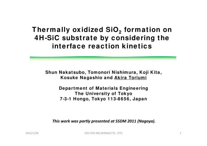
Thermally oxidized SiO 2 formation on 4H-SiC substrate by considering the 4H SiC substrate by considering the interface reaction kinetics Shun Nakatsubo, Tomonori Nishimura, Koji Kita, Shun Nakatsubo, Tomonori Nishimura, Koji Kita, Kosuke
Thermally oxidized SiO 2 formation on 4H-SiC substrate by considering the 4H SiC substrate by considering the interface reaction kinetics Shun Nakatsubo, Tomonori Nishimura, Koji Kita, Shun Nakatsubo, Tomonori Nishimura, Koji Kita, Kosuke Nagashio and Akira Toriumi Department of Materials Engineering Department of Materials Engineering The University of Tokyo 7-3-1 Hongo, Tokyo 113-8656, Japan This work was partly presented at SSDM 2011 (Nagoya). p y p ( g y ) 2012/1/30 IEEE EDS MQ WMNACT31 (TIT) 1
Outline Outline 1 Background and Objective 1.Background and Objective 2 Sample Preparation 2. Sample Preparation 3 Experimental Results 3. Experimental Results 4 Discussion 4. Discussion 5 Conclusion 5. Conclusion 2012/1/30 IEEE EDS MQ WMNACT31 (TIT) 2
Effective WF vs. Vacuum WF Si Si Ge Ge Vacuum level Vacuum level 0 0 ▼ p-type ▲ n-type eV) V) ▲ n type ▲ n-type unction (e unction (e 4 CB 4 CB S=0.27 S 0.02 S = 0.02 ve work fu ve work fu Mg M Yb Y Ti Sc Ni Zr Ti Ni Sc Zr CNL Er Y Er La Hf Au Pt Al VB CNL W W Effectiv Effectiv Al Al Pt Au CNL 4.58eV 5 5 VB 3 3 4 4 5 5 6 6 3 3 4 4 5 5 6 6 Vacuumwork function m (eV) Vacuum work function m (eV) 2012/1/30 IEEE EDS MQ WMNACT31 (TIT) 3
Interface Science of SiC (S 1) Schottky Barrier B M S 1 B S S M 0 Ge Ge Si Si SiC SiC 2012/1/30 IEEE EDS MQ WMNACT31 (TIT) 4
Si Oxidation 2 A t 2 2 2 X Bt 2 A A 4 B O 2 O 2 SiO 2 Si Si B X t A Deal ‐ Grove Model Deal Grove Model 2012/1/30 IEEE EDS MQ WMNACT31 (TIT) 5
Objective To demonstrate high quality SiO 2 /SiC interface i in thermal oxidation process of SiC h l id i f SiC SiO 2 SiO in O 2 SiC SiC SiC SiC 2012/1/30 IEEE EDS MQ WMNACT31 (TIT) 6
Outline Outline 1 Background and Objective 1. Background and Objective 2 Sample Preparation 2.Sample Preparation 3 Experimental Results 3. Experimental Results 4 Discussion 4. Discussion 5 Conclusion 5. Conclusion 2012/1/30 IEEE EDS MQ WMNACT31 (TIT) 7
Kinetic Consideration of SiC Oxidation T ( ゜ C) 1200 1100 1000 900 800 1000 our) Si (Deal & Grove) Deal & Grove, JAP 36 (1965)3770. , ( ) o (nm/h 100 C-face /A ratio 10 Si-face B/ T. Yamamoto et al., JJAP 47 (2008)7803. 1 0.7 0.8 0.9 1.0 1000/T (1/K) Because oxidation process is reaction ‐ limited, its rate is Si > C ‐ face SiC >> Si ‐ face SiC. 2012/1/30 IEEE EDS MQ WMNACT31 (TIT) 8
Kinetic Consideration of SiC Oxidation O 2 O 2 O 2 2 O 2 CO n SiO 2 SiO SiO 2 CO n SiO 2 Si Si SiC SiC SiC Reaction No Reaction 1200 º C 800 º C 2012/1/30 IEEE EDS MQ WMNACT31 (TIT) 9
APL 70 (1997) 2280 APL 70 (1997) 2280. A uniform oxidation on nonplanar SiC by depositing Si prior to SiC oxidation Si Si 70 nm 70 nm SiC SiC Si Oxidation at 1050 º C in Wet O Si Oxidation at 1050 C in Wet O 2 Oxidation of deposited thick Si on SiC in high temperature also causes oxidation of SiC. 2012/1/30 IEEE EDS MQ WMNACT31 (TIT) 10
Sample Preparation Main process flow Wafers Si and C face 4H SiC Si ‐ and C ‐ face 4H ‐ SiC Si d Si deposition(~3 nm) iti (~3 ) 5~6 m epi layer Thermal oxidation / 800 ゜ C, dry O 2 N ‐ dope ~1E16cm ‐ 3 5, 15, 50 min Back metallization (Ni) k lli i ( i) PMA / 940 ゜ C, N 2 , 5 min HfO 2 deposition(~10 nm) PDA / 500 ゜ C, 0.1% O 2 , 30 sec Au electrode HfO HfO 2 SiO 2 Si 4H-SiC NiSix NiSix 2012/1/30 IEEE EDS MQ WMNACT31 (TIT) 11
Why HfO 2 ? 1x10 -10 10 HfO 2 /SiO 2 /Si 8x10 -11 C (F) 6x10 -11 1x10 -10 10 1 kH 1 kHz 10 kHz 8x10 -11 100 kHz 1 MHz 0 -2 -1 0 1 2 V (V) V g (V) No frequency dispersion nor hysteresis No frequency dispersion, nor hysteresis 2012/1/30 IEEE EDS MQ WMNACT31 (TIT) 12
Outline Outline 1 Background and Objective 1. Background and Objective 2 Sample Preparation 2. Sample Preparation 3.Experimental Results 3.Experimental Results 4 Discussion 4. Discussion 5 Conclusion 5. Conclusion 2012/1/30 IEEE EDS MQ WMNACT31 (TIT) 13
Comparison betw een Si-face and C-face SiC - Oxidation Rate - O id ti R t Oxidized at 800 º C Oxidized at 800 º C O 2 1 0 m ︶ n s ︵ s SiO 2 C C S e o n a e c 8 - f i n k c i Si Si h T C S S o n a e c - f i i O O 2 i 6 S SiC SiC SiC ︵ ︶ 0 1 0 2 0 3 0 4 0 5 0 m m Si ‐ C: 0.189 nm O T d a o n e n x t i i i i Si O 0 162 nm Si ‐ O: 0.162 nm Just a monolayer SiO2 if any. Just a monolayer SiO2 if any. Fig. 3 2012/1/30 IEEE EDS MQ WMNACT31 (TIT) 14
Comparison betw een Si-face and C-face SiC - Bi-directional C-V Characteristics - Bi di ti l C V Ch t i ti Si ‐ face C ‐ face 7 - 7 - 5 1 0 x 4 x 1 0 7 - M M 4 1 0 H H x 1 1 z z 7 - 3 3 1 1 0 0 H K H x x K 1 0 0 1 0 0 z z m ︶ 2 ︶ m 2 H K H K c 1 0 1 0 z z / c 7 - / 3 1 0 F x H K H K 1 1 z z F 7 - 2 1 0 x C ︵ 7 - C 2 2 x x 1 1 0 0 ︵ 7 - 1 x 1 0 7 - 1 1 0 x 0 0 0 0 2 1 0 1 2 3 4 2 0 2 4 6 8 1 0 ︵ ︶ ︵ ︶ - - - Ideal V FB V V V V g g Dry oxidation at 800ºC for 50 min Dry oxidation at 800ºC for 50 min On Si ‐ face, there are little frequency dependence and hysteresis, and V FB is close to the ideal value. 2012/1/30 IEEE EDS MQ WMNACT31 (TIT) 15
Outline Outline 1 Background and Objective 1. Background and Objective 2 Sample Preparation 2. Sample Preparation 3 Experimental Results 3. Experimental Results 4.Discussion 4.Discussion 5 Conclusion 5. Conclusion 2012/1/30 IEEE EDS MQ WMNACT31 (TIT) 16
A big difference betw een Si-face and C-face SiC This work 1 0 m ︶ n s s ︵ s C C S e o n a e c 8 - f i n k c i h T C S S o n a e c - f i i O 2 i 6 6 S ︵ ︵ ︶ ︶ 0 1 0 2 0 3 0 4 0 5 0 T. Yamamoto et al., JJAP 47 (2008)7803. T. Yamamoto et al., JJAP 47 (2008)7803. m m m m O O T T d d a a o o n n e e n n x x t t i i i i i i i i Although oxidation rate is significantly different, On Si ‐ face, no carbon will be introduced Into SiO 2 , a same amount of C should be introduced into because of negligible oxidation of Si ‐ face SiC. g g a given thickness of SiO 2 . We can make a carbon ‐ free SiO 2 on Si ‐ face SiC by low temperature oxidation of Si/SiC. 2012/1/30 IEEE EDS MQ WMNACT31 (TIT) 17
Conclusion and Future Outlook • • Good C V characteristics in SiC MOS capacitors have been demonstrated Good C ‐ V characteristics in SiC MOS capacitors have been demonstrated simply by oxidation in dry O 2 at 800 º C, on the basis of thermodynamic and kinetic consideration. • High ‐ k dielectric films will be applicable for SiC gate stacks by using stable interfacial SiO 2 layer. • SiC interface research is old but will be a hot topic. • Si ‐ face is much better than C ‐ face due to a considerably lower oxidation rate in the present method. • MOSFET fabrication and characterization will be the next challenge. 2012/1/30 IEEE EDS MQ WMNACT31 (TIT) 18
Recommend
More recommend
Explore More Topics
Stay informed with curated content and fresh updates.
