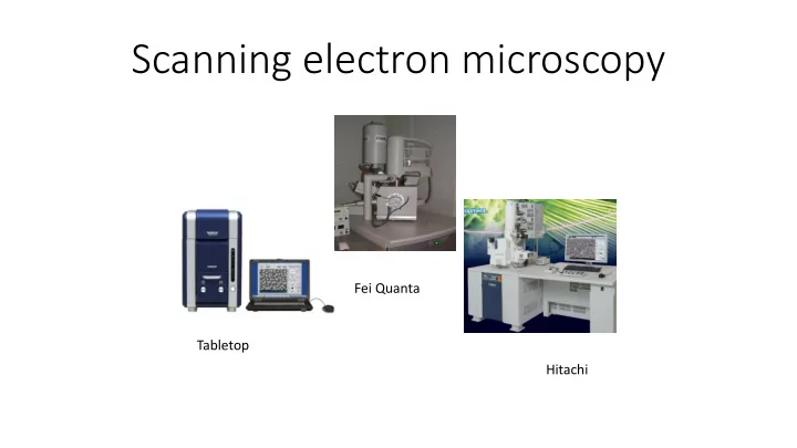
Scanning electron microscopy Fei Quanta Tabletop Hitachi Example: - PowerPoint PPT Presentation
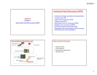
Scanning electron microscopy Fei Quanta Tabletop Hitachi Example: Tin soldier Pb M Sn L EDS analysis Average composition Secondary electrons Backscatter electrons Learning goals: Understanding the principle
Scanning electron microscopy Fei Quanta Tabletop Hitachi
Example: Tin soldier Pb M Sn L EDS analysis – Average composition Secondary electrons Backscatter electrons
Learning goals: • Understanding the principle – Of the instrument – Of type of signals – detectors • Understand how the parameters that you can/must change influences the picture and chemical analysis. • Lab: Demonstration and hands on experience with our three different SEMs – Table top SEM – Environmental SEM – High resolution SEM
Microscopes then and now 1930 1970 2018
Limits to resolution Unaided eye ~ 0.1 mm 0.2 m m Light microscope ~ Scanning EM ~ 1.0 nm Transmission EM ~ 0.1 nm The higher the accelerating voltage, the smaller the wavelength of the electrons and the higher the possible achievable resolution.
Instrument: SEM is it like a TEM ? In SEM, there are several electromagnetic lenses, including condenser lenses and one objective lens. Electromagnetic lenses are for electron probe formation, not for image formation directly, as in TEM. Two condenser lenses reduce the crossover diameter of the electron beam. The objective lens further reduces the cross-section of the electron beam and focuses the electron beam as probe on the specimen surface.
Objective lens Objective lens Cross section The final probe-forming lens has to operate with a relative long working distance (WD= 10 mm), that is the distance between the specimen and lower pole-piece. This is necessary so that the emitted radiation can be collected and detected with desired efficiency. The long working distance increases the spherical aberration of the probe- forming lens, which increases the Final Lens size of the smallest attainable •Probe Forming electron-beam spot. •Labeled as Focus
Objective lens designs Semi-in-lens In lens Out lens Electron beam Electron beam SED SED Electron beam SED Virtual lens SED Virtual lens SED Specimen Specimen Virtual lens Specimen Features Features Features ☆ Ultra high resolution ☆ Ultra high resolution ☆ Easy to observe ☆ High throughput observation ☆ Possible to observe bigger magnetic sample at sample exchange position sample at short WD ☆ Possible to observe ☆ Variety of signal detecting ☆ Variety of signal detecting bigger sample system to optimize the contrast system to optimize the contrast ☆ Topographical imaging ☆ Deep depth of Focus
Compare the three different designs of objective lens : 1:Conventional lens Here the magnetic field of the lens is located inside the lens and the specimen sits away from the field. This leads to that the beam travels “unprotected” between lens and sample and is more vulnerable to EM disturbance. On the other hand the distance between lens and specimen only has limited effect on the signal strength. 2: Snorkel lens, semi-in-lens or immersion lens Here the magnetic field is projected down below the lens to enclose the specimen if it is located at short working distance. At the same time as the beam is protected from EM disturbance the electrons are effectively captured and led up through the lens to be detected by an in-lens detector. For longer working distance or when a side illumination effect is wanted, a classical SE detector is mounted in the chamber. 3: In-lens Here the sample sits on a TEM-type holder and has a maximum size of ca. 4x4x9 mm. Benefits here are excellent mechanical stability, high electron collection efficiency and very high EDS count rates.
Relationship between resolution and focal length
Different e - sources and gun types W LaB 6 Schottky FE Cold FE 1 – 2 m m 1 – 2 m m Source size 10 – 25 nm 3 - 5 nm 2300 C 1500 C 1500 C Temperature Room temp Brightness 1 10 500 1000 [A/cm 2 sr] 1x10 6 1x10 7 5x10 8 2x10 9 Energy 2.0 eV 1.5 eV 0.5 eV 0.2 eV spread, E Stability,%/h 0.1 % 0.2 % 0.2 % 2-3 % 50 nA -1 m A 50 nA -1 m A Probecurrent >100 nA 20-30 nA Life time 1 month 6 months 18 months > 5 years 10 -5 Torr 10 -7 Torr 10 -9 Torr 10 -11 Torr Gun vacuum
Magnification of SEM is determined by the ratio of the linear size of the display screen to the linear size of the specimen area being scanned. The linear magnification is given by Electronbeam is scanned across the specimen and the procedure is known as Raster scanning. Raster scanning causes the beam to sequentially cover a rectangular area on the specimen. The signal electrons emitted from the specimen are collected by the detector, amplified and used to reconstruct the image according to one-to-one correlation between scanning points on the specimen and picture points on the screen of cathode ray tube (CRT). CRT converts the electronic signals to a visual display.
Condenser Lens Current and Resolution. The current in the condenser lens changes the spot size or diameter of the beam of electrons that scans the sample. More detailed information will be collected when the electron beam scans the same area with a smaller spot size. An increased current or a higher number for the condenser lens (CL) setting, will produce a smaller spot size and in general will result in a better resolution (A).
Diatome Courtesy of Gokhan Taken by Quanta SEM microscope Magnification: 30000x Sample: Diatome Detector: ETD Voltage: 4.0kV Vacuum: 4.01e-4Pa Horizontal Field Width: 9.93 μ m Working Distance: 7.7 Spot: 2.0 https://www.fei.com/image-gallery/ Same picture - different size Magnification ?
Beam samples interaction:
Scattering “Inelastic” scattering refers to a variety of physical processes that act to progressively reduce the energy of the beam electron by transferring that energy to the specimen atoms through interactions with tightly bound inner-shell atomic electrons and loosely bound valence electrons. Although the various inelastic scattering energy loss processes are discrete and independent, Bethe (1930) was able to summarize their collective effects into a “continuous energy where E is the beam energy (keV), Z is the atomic number, ρ is the density (g/cm3), A is the atomic weight (g/mol), and J is the “mean ionization potential” (keV) given by
Beam interaction volumes Sample = Si 1μm Vacc : 10kV Vacc : 1kV Images are formed because of beam interaction with the sample This happens in a volume, not in a point The size of this volume varies with beam energy...
Beam Excitation Volumes
Elastic scattering Simultaneously with inelastic scattering, “elastic scattering” events occur when the beam electron is deflected by the electrical field of an atom (the positive nuclear charge as partially shielded by the negative charge of the atom’s orbital electrons), causing the beam electron to deviate from its previous path onto a new trajectory, as illustrated schematically in the figure. The elastic scattering crossection, can be used to estimate how The mean free path is of the order of nm. far the beam electron must travel on average to experience an Elastic scattering is thus likely to occur hundreds to elastic scattering event, a distance called the “mean free path,” thousands of times along a Bethe range of several hundred to λ several thousand nanometers.
Accelerating voltage
Signals in the SEM Electron beam 一 一 SE High energy BSE (I) Inner information 一 一 SE SE II Low energy BSE (II) SE I Surface information 一 一 一 一 一 一 一 Z 一 一 SE escape depth 一 sample 一 一 Z 一 一 BSE escape depth SE
Emitted electrons (SE) (BSE) Secondary electron Back scattered electron Electron amount 50eV 1 10 100 10000 1000 Energy of signal electron (eV) (Notice that the scale is logarithmic) When a sample is hit by an electron beam a variety of electron emissions are available.
“ Huskelapp ” The group of secondary electrons (SE) can be divided into 4 groups. There are SEI, SEII, SEIII, and SEIV. These electrons are classed according to how they are generated. A SEI is an electron is an electron that is generated at the point of primary beam impingement in surface of the specimen. Thus, it carries the highest resolution information. A SEII is an electron that is generated when a backscattered electron leaves the surface of the specimen. Due to the energy of backscattered electrons, this SEII could leave the surface of the specimen microns away from the primary beam impingement site. SEIIs hurt the resolution of the image, but add greatly to overall image brightness. A SEIII is an electron released when an energetic backscattered electron strikes the interior of the specimen chamber, causing a SE to be released. SEIVs are formed when the primary beam strikes an aperature within the electron column. SEIIIs and SEIVs contribute noise to the image. By understanding signal formation, the specimen can be properly prepared for analysis.
SE yield variation The rapid change in the incident electron beam range causes a large, characteristic variation in the SE yield Typically the yield rises from ~0.1 at 30keV to in excess of 1 at around 1keV, and as high as 100 for some materials Experimental SE yield data for Ag
Recommend
More recommend
Explore More Topics
Stay informed with curated content and fresh updates.
