Scanning electron microscopy methods in study of micro objects - PowerPoint PPT Presentation
Scanning electron microscopy methods in study of micro objects Members : Ana-Maria Panaitescu Iuliana Taran University of Bucharest,Faculty of Physics Supervisor: Orelovich Oleg JINR Laboratory: FLNR Scanning electron
Scanning electron microscopy methods in study of micro objects Members : Ana-Maria Panaitescu Iuliana Taran University of Bucharest,Faculty of Physics Supervisor: Orelovich Oleg JINR Laboratory: FLNR
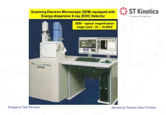
Scanning electron microscope-principles A scanning electron microscope (SEM) is a type of electron microscope that produces images of a sample by scanning it with a focused beam of electrons. The electrons interact with atoms in the sample, producing various signals that contain information about the sample's surface topography and composition. The electron beam is generally scanned in a raster scan pattern, and the beam's position is combined with the detected signal to produce an image. SEM can achieve the best resolution around 1 nanometer. Specimens can be observed in high vacuum, in low vacuum, in wet conditions (in environmental SEM), and at a wide range of cryogenic or elevated temperatures.
SEM principle/Signals available from specimen
All samples must be of an appropriate size to fit in the specimen chamber and are generally mounted rigidly on a specimen holder called a specimen stage. Several models of SEM can examine any part of a 6-inch (15 cm) semiconductor wafer, and some can tilt an object of that size to 65 ° . During the process of using the SEM it is possible to observe that the samples consist of different materials. In case the non-conductive specimen is investigated it is necessary to cover it with conductive layer . There are three general reasons for this operation: -the surface of sample must be electro conductive to minimize charging from initial beam; - the surface of sample must be thermo conductive to minimize local heating (as result of high density current in the influence area); -the material of sample must have high atomic number to increase the coefficient of secondary electron emission. First and second items can be assured by carbon layer on the sample surface. But a lot of secondary electrons can be provided from element with high number of electrons on the outer atomic levels (for example Cu, Ag, Au, Pt). In accordance to all these reasons the gold or platinum layers are most preferable.
The most special features of this scanning electron microscope are that it is truly a tabletop SEM, it is portable and it is designed for minimal preparation of specimens. The microscope is lightweight by design. The HITACHI TM3000 requires also low energy, just 550W. The HITACHI TM3000 is used for normal sized specimens. Characteristics Accelerating voltage: 5 or 15 kV, tungsten source Magnification: X 15 to X 30,000 30 nm resolution Backscattered detector only Charge reduction mode (which uses higher chamber pressure) allows imaging of uncoated samples Easy to use and portable
Instrument Specifications The Hitachi S-3400N SEM is a high performance, user-friendly scanning electron microscope with new improvements that allow the best results for a wide range of applications. Features include: Resolution -3.0nm High Vacuum Mode; -4.0nm Variable Pressure Mode. Chamber -Accomodates 10 inch specimen. Electron Gun -Variable Quad Bian Circuitry with Secondary Electrons (SE) Accelerator Plate Detectors-SE (Secondary Electrons); -BSE (Backscattered Secondary Electrons); -2 X-Ray detectors.
General Description: The Q150R system is a versatile magnetron sputter coater/carbon evaporator for preparing specimens for examination by electron microscopy. Q150R can be used to: Sputter coat samples using targets such as Gold or Platinum. Evaporate carbon support films for X-Ray analysis and conducting coatings for SEM using carbon cords. Glow discharge. We have used Q150R ES which is a combined system with interchangeable inserts for sputter coating or carbon evaporation. The instrument is fully adaptable to a wide range of specimens and offers easy loading and unloading of samples.
Standard sample for calibrating a microscope Sample:Planotec Sillicon test specimen mount C.
Calculus of parameteres of the membrane; the number of pores (the glossy side of a polymer foil ) Task: Capturing the image with the proper magnification that allows us to calculate the parameters of 300-400 pores in order to calculate the density of pores.
The neccessity of using a conductive layer Comparison between sample with Au layer and sample without Au layer without gold
Polymer foil:polycarbonate Aim : to investigate the behaviour of foil with different structure on 2 sides - matte side and glossy side
Investigation of Z-contrast Carbon tape Gold layer Copper band Specimen stage
Cross section of a sample mounted on a special specimen stage Normal specimen stage Special specimen stage
Cross section of a sample mounted on a different specimen stage
Investigating salt particles on carbon tape (HITACHI TM3000) Salt particle on carbon tape salt crystals on carbon tape Salt particle on carbon tape
Investigating salt particles on carbon tape (HITACHI TM3000) Salt crystals on carbon tape Salt crystals on carbon tape
Investigating salt powder on carbon tape (HITACHI S 3400 N)
Investigation of natural dark hair
Investigation of blonde dyed hair Black part
Investigation of blonde dyed hair Black part
Investigation of an eyelash
Investigation of mascara eyelash
The use of gonyometre for the investigation of relief features 30 ° tilt 60 ° tilt The general view of the sample surface area
Scanning electron microscopy is widely employed to determine the structural characteristics of various materials like crystals, amorphous materials, polymers and microfiltering membranes. • Comprehensive information on the membrane structure can be obtained by analyzing the images of both the membrane surfaces and cross sections. Electron microscopy is helpful for offering information regarding the elemental composition by collecting the X-Ray characteristic radiation spectrum.
Thank you for your attention!
Recommend
More recommend
Explore More Topics
Stay informed with curated content and fresh updates.
