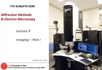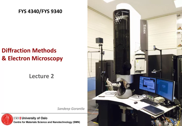
Diffraction Methods & Electron Microscopy Lecture 2 Sandeep - PowerPoint PPT Presentation
FYS 4340/FYS 9340 Diffraction Methods & Electron Microscopy Lecture 2 Sandeep Gorantla 1 FYS 4340/9340 course Autumn 2016 Transmission Electron Microscopy Introduction and Basics Part- 1 Sandeep Gorantla 2 FYS 4340/9340 course
FYS 4340/FYS 9340 Diffraction Methods & Electron Microscopy Lecture 2 Sandeep Gorantla 1 FYS 4340/9340 course – Autumn 2016
Transmission Electron Microscopy Introduction and Basics Part- 1 Sandeep Gorantla 2 FYS 4340/9340 course – Autumn 2016
Learning more about TEM! Courtesy : WWW.amazon.com 3 FYS 4340/9340 course – Autumn 2016
Learning more about TEM! http://www.matter.org.uk/tem/ 4
Learning more about TEM! 5
Why learn about Transmission Electron Microscopy (TEM)? 6 FYS 4340/9340 course – Autumn 2016
7 FYS 4340/9340 course – Autumn 2016
Role of TEM in Materials Science Research and Development Solving Materials Science problems/mysteries by probing analytically and understanding structure-property relationships at atomic scale level Materials Science Paradigm Courtesy : www.wikipedia.com 8 FYS 4340/9340 course – Autumn 2016
Allotropes of carbon graphene graphite fullerene nanotube (Courtesy: The Royal Swedish Academy of Sciences) 9 FYS 4340/9340 course – Autumn 2016
10 Courtesy : www.extremetech.com
Courtesy : Knut Urban, Nature Materials 10, 165 – 166 (2011) 11
1D nanomaterials modification in TEM - Irradiation of solids with energetic particles usually leads to damage - However, in the case of carbon nanostructures, electron irradiation was observed to have some beneficial effects (a) Irradiation – mediated engineering (b) self-assembly or self-organization Courtesy : Krasheninnikov, A. V. et al., Nature Mater., 6, 723 (2007) 12 FYS 4340/9340 course – Autumn 2016
13 FYS 4340/9340 course – Autumn 2016
14 FYS 4340/9340 course – Autumn 2016
Interface: defects on outer-wall of a nanotube and fullerene Courtesy : Gorantla, S. et al., Nanoscale, 2, 2077 (2010) 15 FYS 4340/9340 course – Autumn 2016
Interface: defects on outer-wall of a nanotube and fullerene Nanohump formation (Covalent interactions of fullerene fusion) Movie Settings: • Frame speed: 0.6 s • Total Frames: 48 Experimental conditions: • Acquisition time: 1 s • Time gap between individual frames : 1s - 30s • Total time: 14 mins Courtesy : Gorantla, S. et al., Nanoscale, 2, 2077 (2010) 16 FYS 4340/9340 course – Autumn 2016
Interface: defects on the outer-wall of a SWCNT and fullerene Fullerene fusion with a nanohump (Covalent interactions of fullerene fusion) Movie Settings: • Frame speed: 0.6 s • Total Frames: 48 Experimental conditions: • Acquisition time: 1 s • Time gap between individual frames : 1 s Courtesy : Gorantla, S. et al., Nanoscale, 2, 2077 (2010) 17 FYS 4340/9340 course – Autumn 2016
HETEROSOLAR PROJECT The aim of the work Develop new solar cell devices base on ZnO/Cu 2 O heterojunctions coupled with convetional Si based solar cells Properties determined by the structures, faults and interfaces. TCO Cu 2 O ZnO n-type * Theoretical eficiency ~20 % 2.17 eV 3.4 eV * Highest exp. eficiency 1-4 % p-type Si 18 Sub project : (S)TEM to characterize the thin films and their interfaces.
Cu 2 O (sputtering, 300nm) Cu 2 O ZnO Single Crystal Cu 2 O CuO ??? ZnO 50 nm ZnO 1 nm 19 FYS 4340/9340 course – Autumn 2016
CuO ZnO 20 FYS 4340/9340 course – Autumn 2016
Transmission Electron Microscope Brief History 21 FYS 4340/9340 course – Autumn 2016
Brief History: The first electron microscope Ernst Ruska: Nobel Prize in physics 1986 • Knoll and Ruska, first TEM in 1931 • Idea and first images published in 1932 • By 1933 they had produced a TEM Electron Microscope Deutsches with two magnetic lenses which gave Museum, 1933 model 12 000 times magnification. 22
Brief History: The state-of-art TEM Electron Microscope Deutsches Museum, 1933 model FEI Titan 60-300 TEM, NORTEM facility- UiO Installed: 2014 23
Brief History: The state-of-art TEM BIG LEAP : Introduction of Lens Aberration Correctors allowing atomic resolution at low accelerating voltages. Resolution limit Before C s correction Year Resolution 1940s ~10nm 1950s ~0.5-2nm 0.3nm (transmission) Typical TEM operating voltages 1960s in Materials Science Research ~15-20nm (scanning) 300 kV 0.2nm (transmission) 1970s 200 kV After C s correction 7nm (standard scanning) 80 kV 0.15nm (transmission) 60 kV 1980s 5nm (scanning at 1kV) 0.1nm (transmission) 1990s 3nm (scanning at 1kV) 2000s <0.1 nm (Cs correctors) Core of the M100 galaxy seen through Hubble (source: NASA) Courtesy : http://www.sfc.fr/Material/hrst.mit.edu/hrs/materials/public/ElecMicr.htm 24 FYS 4340/9340 course – Autumn 2016
Transmission Electron Microscope Fundamentals 25 FYS 4340/9340 course – Autumn 2016
Electrons interaction with the specimen Electrons have both wave and particle nature Typical specimen thickness ~ 100 nm or less Typical TEM operating voltages in Materials Science Research 300 kV 200 kV 80 kV 60 kV Courtesy : D.B. Williams & C.B. Carter, Transmission electron microscopy 26 FYS 4340/9340 course – Autumn 2016
Electron lenses Any axially symmetrical electric or magnetic field have the properties of an ideal lens for paraxial rays of charged particles. F= -eE • Electrostatic – Not used as imaging lenses, but are used in modern monochromators • ElectroMagnetic F= -e(v x B) – Can be made more accurately – Shorter focal length Courtesy : http://www.matter.org.uk/tem/lenses/electromagnetic_lenses.htm 27 FYS 4340/9340 course – Autumn 2016
TEM Lens Aberrations • Spherical aberration coefficient r 2 d s = 0.5MC s α 3 r 1 α M: magnification C s :Spherical aberration coefficient α: angular aperture/ angular deviation from optical axis Disk of least confusion Spherical aberration x y-focus v - Δ v y x-focus v Astigmatism Chromatic aberration 28 FYS 4340/9340 course – Autumn 2016
TEM Lens Aberrations Schematic of spherical aberration correction Courtesy : Knut W. Urban, Science 321, 506, 2008; CEOS gmbh, Germany; www.globalsino.com 29 FYS 4340/9340 course – Autumn 2016
TEM Lens Aberrations Why we need an aberration-corrected TEM at 80kV??? -Correcting aberrations improves the TEM resolution at 80 kV Uncorrected 80 kV ~ 0.3 nm (Courtesy : NASA) Corrected 80 kV ~ 0.14 nm - Improved resolution enables the possibility of imaging carbon nanostructures at atomic level Uncorrected 80 kV Aberr. corrected 80 kV 30 FYS 4340/9340 course – Autumn 2016
Transmission Electron Microscope Instrumentation – Part 1 31 FYS 4340/9340 course – Autumn 2016
FEG gun Extraction Anode Gun lens Monochromator Aperture Monochromator Accelerator Gun Shift coils C1 aperture/mono energy slit C1 lens C2 lens C2 aperture Condenser alignment coils C3 lens C3 aperture Beam shift coils Mini condenser lens Objective lens upper Specimen Stage Objective lens upper Image Shift coils Objective aperture Cs Corrector SA Aperture Diffraction lens Intermediate lens Projector 1 lens Projector 2 lens HAADF detector Viewing Chamber Phosphorous Screen BF/CCD detectors EELS prism GIF CCD detector Courtesy : David Rassouw, CCEM, Canada 32 FYS 4340/9340 course – Autumn 2016
Electron gun Illumination system Specimen stage Imaging system Projection and Detection system Courtesy : David Rassouw 33 FYS 4340/9340 course – Autumn 2016
FEG Electron gun source 34 FYS 4340/9340 course – Autumn 2016
Specimen Stage 35 FYS 4340/9340 course – Autumn 2016
TEM Specimen Holder 36 FYS 4340/9340 course – Autumn 2016
TEM Specimens • Typically 3 mm in diameter Courtesy: http://asummerinscience.blogspot.no 37 FYS 4340/9340 course – Autumn 2016
TEM Viewing Chamber – Phosphorous Screen 38 FYS 4340/9340 course – Autumn 2016
TEM Image recording CCDs and EELS Spectrometer 39 FYS 4340/9340 course – Autumn 2016
Transmission Electron Microscopy Introduction and Basics Part-2 40 FYS 4340/9340 course – Autumn 2016
TEM in Materials Science The interesting objects for TEM is not the average structure or homogenous materials but local structure and inhomogeneities Defects Interfaces Chemical composition Precipitates Chemical bonding Atomic Structure Electronic Structure 41 FYS 4340/9340 course – Autumn 2016
TEM techniques Main Constrast phenomena in TEM Imaging • Mass thickness Contrast Conventional TEM Bright/Dark-Field TEM • Diffraction contrast High Resolution TEM (HRTEM) • Phase Contrast Scanning TEM (STEM) Energy Filtered TEM (EFTEM) • Z-contrast Diffraction Phase identification, defects, orientation Selected Area Electron Diffraction relationship between different phases, nature of Convergent Beam Electron Diffraction crystal structure (amorphous, polycrystalline, single crystal) Spectroscopy Chemical composition, electronic states, nature Electron Dispersive X-ray Spectroscopy (EDS) of chemical bonding (EDS and EELS). Electron Energy Loss Spectroscopy (EELS) Spatial and energy resolution down to the atomic level and ~0.1 eV. 42 FYS 4340/9340 course – Autumn 2016
Recommend
More recommend
Explore More Topics
Stay informed with curated content and fresh updates.
