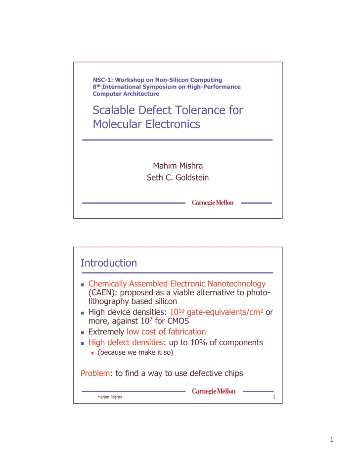
Scalable Defect Tolerance for Molecular Electronics Mahim Mishra - PDF document
NSC-1: Workshop on Non-Silicon Computing 8 th International Symposium on High-Performance Computer Architecture Scalable Defect Tolerance for Molecular Electronics Mahim Mishra Seth C. Goldstein Introduction Chemically Assembled Electronic
NSC-1: Workshop on Non-Silicon Computing 8 th International Symposium on High-Performance Computer Architecture Scalable Defect Tolerance for Molecular Electronics Mahim Mishra Seth C. Goldstein Introduction � Chemically Assembled Electronic Nanotechnology (CAEN): proposed as a viable alternative to photo- lithography based silicon � High device densities: 10 10 gate-equivalents/cm 2 or more, against 10 7 for CMOS � Extremely low cost of fabrication � High defect densities: up to 10% of components � (because we make it so) Problem: to find a way to use defective chips Mahim Mishra 2 1
Using defective chips � Use redundancy, as in memory chips � defect rates in CAEN devices too high � does not work for logic � Use fault-tolerant circuit designs � large overheads (space and time) � needs hard upper bound on number of faults � circuit design is difficult � Compose the fabrics of regular, repeating structures and use reconfiguration We will use this last approach Mahim Mishra 3 Defect tolerance through reconfiguration � Solution: suggested by reconfigurable FPGAs and Teramac custom computer � Post-fabrication testing phase: locates and maps all defects � Configurations routed around the defects � Manufacturing time complexity traded-off for post- fabrication programming We will call reconfigurable, CAEN based fabrics nanoFabrics Mahim Mishra 4 2
Routing around a defect Mahim Mishra 5 Requirements for testing � The testing method used should not require access to individual fabric components � It should scale with the number of defects � It should scale with fabric size Testing should not become a bottleneck in the manufacturing process Mahim Mishra 6 3
Talk overview � Introduction and motivation � Our proposed solution � scaling with defect density � scaling with fabric size � Simulations and Results � Open Issues � Conclusions Mahim Mishra 7 Testing method: overview � Test circuits implementing a chaotic mathematical function � Incorrect circuit output => defect! � Correct circuit output => all its components are marked defect-free. � Similarities with the counterfeit coin problem � however, they only find one coin! � More importantly, group testing Mahim Mishra 8 4
Group testing � Testing strategy which identifies +ves in a population by testing a group at a time � Used for a wide-range of problems: � blood tests, product tests, multiple-access communication � more recently, in computational biology � Has both adaptive and non-adaptive versions � Constraints considered so far are different from ours � fewer number of +ves � possible to test individual members of population Mahim Mishra 9 Testing method: overview � When are results analysed? � Are tests adaptive or non-adadptive? Mahim Mishra 10 5
Test-circuits in action Mahim Mishra 11 Some terminology � n components being tested � Probability of defect p � Each test circuit has k components � Circuits arranged in various orientations, or tilings � % of good components recovered: yield In the example, � n =25 � k =5 � 2 tilings � yield is 100%. Mahim Mishra 12 6
Assumptions � Permanent defects � defective component always displays faulty behavior � defect in one component does not affect others � i.e., no short-circuits or stuck-at defects between wires � manufacturing process biased to ensure this � no Byzantine failures � Defects in inter-connects: similar to defects in ordinary components Mahim Mishra 13 Assumptions (cont.) � Arbitrary, unlimited connectivity � any component can be connected to any other, including non-adjacent ones � makes large number of tilings possible � Above assumption: to simplify analysis Mahim Mishra 14 7
Scaling with defect density � Expected k*p defects/test-circuit � Fewer defects/circuit: easier to locate � We examine the following 3 cases: � k*p « 1 � k*p ≈ 1 � k*p » 1 � Remember, k cannot be too small Mahim Mishra 15 Low defect rates: k*p « 1 or k*p ≈ 1 � Many test circuits have no defects � Testing strategy: � configure test-circuits using a particular tiling � if any circuit’s output is correct, mark all components defect-free � repeat for many tilings � Points to note: � tests are non-adaptive: all tilings known beforehand � no test-time “place-and-route” needed Mahim Mishra 16 8
Example with very low defect rate Mahim Mishra 17 Example with higher defect rate Mahim Mishra 18 9
Tilings required for low defect rates Desired yield = 99% Mahim Mishra 19 High defect rates: k*p » 1 � Many defects/test-circuit � Finding a defect free circuit is extremely unlikely � e.g., for k=100, p=0.1, probability of finding a defect- free circuit = 1.76*10 -5 � The previous approach does not work: something new is needed Mahim Mishra 20 10
How can so many defects be located? � Make k smaller � k*p is close to 1 � may not be possible: no fine-grain access to components � increases test time � Make the tester highly adaptive � tight feeback loop � result of each test determines configuration of next tester � will make testing very slow � Use more powerful test circuits! Mahim Mishra 21 Making test circuits more powerful � Use test-circuits which count defects � error in output depends directly on number of defects � e.g., use error-correcting, fault-tolerant circuit designs � These can return correct counts only upto a certain threshold � must indicate when threshold is crossed � use two different test circuits simultaneously! Mahim Mishra 22 11
New testing methodology � Split into two phases: � probability-assignment phase � defect-location phase � First phase: identifies components with high probability of being defect-free � Second phase: tests these components further to pin-point defects � each phase: uses many different tilings Mahim Mishra 23 Probability-assignment phase � Each component made a part of many different test circuits and defect counts are obtained � Find probability of each component being good using Bayesian probabilistic analysis � Discard components with low probability of being good Mahim Mishra 24 12
This works, but why? � Intuitively, a defective component increases defect counts of all circuits it is a part of � If a component is part of many circuits with a high defect count, our analysis assigns it a low probability of being good � Precise mathematical model of this process: still under development Mahim Mishra 25 Defect location phase � Remaining components have low defect rate � Configure into test circuits, mark all the components good if circuit has no defects � Repeat for many different tilings � Everything left is marked bad Mahim Mishra 26 13
Simulations � For cases with low defect rates, � test-circuits gave 0-1 answers � measured yields for different number of tilings � For cases with high defect rates, � test-circuits counted defects upto a certain threshold � measured yields obtained for different counting thresholds and different error rates Mahim Mishra 27 Simulations with low defect densities Number of Expected Achieved Tilings t Yield % Yield % 1 91.36 91.34 k =11 p =0.009 2 99.25 99.29 1 38.94 38.05 2 62.72 62.05 k =11 p =0.09 5 91.51 91.17 10 99.28 99.24 Mahim Mishra 28 14
Simulations with high defect densities here, k=101, tilings used = 101 Mahim Mishra 29 Scaling with fabric size � Each k*k piece of fabric requires � O(k) tilings � therefore, O(k) testing time � Configure tested parts themselves as testers � reduces time on external tester � Configure multiple testers simultaneously � Wave-like progress of testing: total time needed is square root of fabric size Mahim Mishra 30 15
Open issues � Accounting for limited fabric connectivity: � we assume unlimited fabric connectivity � actual connectivity: will require lesser number of tilings � Using less restricted tilings: � scalability of probability calculations needs to be checked � Accounting for real defect types and distributions: � Byzantine defects � clustered defects � particular defect types such as stuck-at defects Mahim Mishra 31 More open issues � Exploring usability of alternative circuit types: � Defect-counting circuits may be unrealizable � however, different, less powerful test circuits might also give useful information � Test circuit design: � designing test circuits that satisfy our requirements will be a non-trivial task � Developing mathematical model of probability- assignment phase Mahim Mishra 32 16
Conclusions � CAEN-based computing fabrics with high defect densities can be used if we locate the defects and configure around them � To locate these defects, it is possible to devise a testing method which is scalable and has a high yield � Such a scalable testing method will require more powerful test circuits than are used currently. Mahim Mishra 33 Low defect rates: analysis � If the desired yield is y and the number of tilings required to achieve this is t , � For k =10 and p =0.01, a yield of at least 99% can be achieved with t =2, i.e., with only 2 tilings. Mahim Mishra 34 17
Recommend
More recommend
Explore More Topics
Stay informed with curated content and fresh updates.



![CS184c: Computer Architecture [Parallel and Multithreaded] Day 16: May 31, 2001 Defect and](https://c.sambuz.com/1019509/cs184c-computer-architecture-parallel-and-multithreaded-s.webp)


