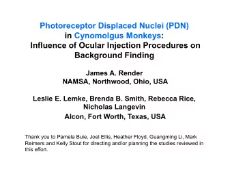
Principles of Power Integrity for PDN Design: Larry Smith Eric - PowerPoint PPT Presentation
PDNpowerIntegrity.com Principles of Power Integrity for PDN Design: Larry Smith Eric Bogatin Principal Power Integrity Engineer Signal Integrity Evangelist larry.smith@pdnpowerintegrity.com eric@bethesignal.com Copies of this presentation
PDNpowerIntegrity.com Principles of Power Integrity for PDN Design: Larry Smith Eric Bogatin Principal Power Integrity Engineer Signal Integrity Evangelist larry.smith@pdnpowerintegrity.com eric@bethesignal.com Copies of this presentation are available on the Signal Integrity Academy web site: www.beTheSignal.com, Videos, Recorded Presentations, Webinars Course, section 60
Recent Publication from Larry and Eric Most of this tutorial is covered in book − Chapter 4: Inductance and PDN Design − Chapter 5: MLCC capacitors − Chapter 8: PDN Ecology − Chapter 9: Transient Currents − Chapter 10: PDN Resonant Calculator 2
Agenda – Principles of Power Integrity for PDN Design The “Scope” of the Power Distribution Network (PDN) Target Impedance, PDN Topology and Transient Current Introduction Capacitance, Inductance and Resistance, and PDN Ecology Transient Currents – more details VRM, Switched Capacitor Load and PDN Resonant Calculator Measurements, Frequency and Time Domain Measurements and PDN Correlation 3
Why Do we Care? One Example: Vdd Self Aggression Noise: problem and root cause PDN 500 MHz clock Z PDN Core PDN voltage noise– 200mv/div Z chip Vdd chip VRM The root cause Period of each clock 350ps • 500 MHz clock (2 nsec period) • Multiple drivers drawing current through PDN at 1 100ps jitter/vertical div Gbps, PRBS • PDN noise causes clock jitter ~ 1 psec/mV Courtesy of Altera 4
Why PDN Design is Confusing What’s an elephant? …it depends ...on what is important to you • Is it VRM noise? VRM stability? • Is it decoupling capacitor selection? • Is it cavity noise due to signals switching return planes? • Is it noise on the I/O rails? • Is it noise on the PLL or ADC rails? 5
What is the PDN? ( Self) consumption Generation (pollution ) distribution From the die’s perspective From the VRM’s perspective 60 inches 1 600 inches inches 10 f MHz Impedance (mOhms) VRM Bulk cap SMT caps ODC 1 kHz 10 kHz 100 kHz 1 MHz 10 MHz 100 MHz 1 GHz 6
> 4 orders of Magnitude in Current Load Max Power Power current generation consumption per rail Multi-phase Server class 100 A Buck Power sequencing Motherboards 10 A Buck-boost Automotive Power management IC 1 A Consumer Linear Portable/wireless Low Drop Out 0.1 A Embedded Battery Boost Wearable Energy harvesting Internet of Things 7
Classification of PDN Loads IO – Jitter is important − DDR − Serdes − General Purpose IO Logic Cores – Fmax, Vmin, voltage droops are important − Microprocessors − Graphics Processors − Modem 8
Why PDN Design is so Confusing: It’s not just 1 problem and root cause, it’s 12 Self aggression noise From VRM on VRM From Vcc on Vcc From Vdd on Vdd VRM From signals on signals (discontinuities) Signals “Pollution” of the board/pkg interconnects From VRM From I/O Vcc- I/O From core From signals • Mutual aggressors: cross talk coupling from the PDN Vdd- core • To VRM • To I/O Board level PDN • To core interconnects • To signals 9
Putting the PDN in perspective: Target Impedance, PDN Topology and Transient Currents Larry Smith
Target Impedance Definition Based on Ohms Law Two easily understood and difficult to obtain parameters − Tolerance Vdd tolerance 1.2 V 0.05 Z 10 mOhm − Transient current target I I 7 A 2 A max min − Expressed as percentage of maximum current Target impedance is a function of frequency if − Tolerance is a function of frequency Supply that meets Z target almost − Transient current is a function of frequency certainly will not exceed specified voltage tolerance with given transient current … but that can be expensive … 11
Components for Power Distribution Network (PDN) 12
PDN Space: Very Low Currents to Very High Currents PDN principles are still the same: Manage the PDN impedance Target Impedance Scales It is just a version of Ohms Law Z target IOT Mobile Product Current Z target Servers Internet of Things mA Ω Mobile Amps m Ω Computing 0.001 1 1000 Current in Amps µ Ω Servers 100’s of amps Vdd tolerance 1.2 V 0.05 Z 10 mOhm target I I 7 A 2 A max min 13
Jitter Is Important for IO and Serdes Applications Voltage droops are important for logic cores − Determines Fmax – maximum clock frequency − Determines Vmin – minimum functional voltage IO and Serdes Applications − Sensitive to dV/dt − PDN induced Jitter PRBS Clock gating − Creates PDN current at resonant frequency − Excessive PDN noise: 300 mV p-p − 350 ps jitter correlates to PDN noise PDN noise needs to be controlled for both logic cores 50 ns / div and communications circuits 14
Transient Current Considerations Transient current paradox − Commonly used terminology − But often misunderstood… Examples of Transient current − Impulse: Clock edge current − Step: Burst transient − Resonance: Periodic burst transient I transient = I max – I min = dI Current waveforms have large variation across system − Filtering effect of inductance and capacitance − Very different time constants Current profiles have frequency content depending on length of time, dT − 100’s of pSec only affects die − Few nSec affects package − 10’s of nSec affects PCB − µSec affects VRM 15
Current Definitions – On-Chip Level 70 Clock 60 Clock edge current: 50 Clock Edge − Instantaneous current drawn Current [A] Current 40 Area is − by die logics at clock edges 30 Dynamic charge Current per cycle Charge per clock cycle: 20 10 − Independent of clock frequency T 0 0 2 4 6 8 10 Q i ( t ) dt Time [ns] clk _ edge 70 0 Dynamic current: 60 unchanged − Time averaged clock edge current 50 Current [A] 40 − Comes with the clock 30 − Static (leakage) current not included doubled 20 − Used for target impedance design 10 − Proportional to clock frequency 0 0 2 4 6 8 10 Time [ns] 1 T I Q / T i ( t ) dt dynamic clk _ edge T 0 16
Time Average Dynamic Current System level current considerations Low Activity: Clock Edge Current − Clock is active but Data is Idle High Activity High Activity: Low Activity Low Activity Transient Current − Clock and Data are active Transient Current: − high-activity current minus low-activity current − AKA power transient System Level PDN responds to power transients. Clock edge currents are filtered by the package. 17
L, R and C in the PDN, PDN Resonance Calculator Larry Smith
System Cross Section for Measurements die package PCB decap Die on Package on PCB Core Sense PCB Capacitance is mostly on the die Inductance is mostly in the package and PCB Resistance is in the die, package, PCB and capacitors Simple RLC circuit closely represents system Next we will examine lab measurements for a real hardware system 19
Fundamental PDN Voltage Responses Impulse Response Resonance Step Response (Clock Edge Noise) Response 10 nS / Div 10 nS / Div 10 nS / Div Waveforms curtesy of Altera. On-Chip PDN Noise Characterization and Modeling, DesignCon 2010 20
Equations for Series and parallel circuits Measure series resonance from the package balls Stimulate parallel resonance from chip circuits The RLC elements are the same 1 f Estimate of impedance peak at resonance Resonant frequency 0 2 LC 2 X L C / Z Z Q factor - L Reactance at resonance peak 0 R R X Z 0 C Z L C / The beginning of a PDN Resonant Calculator 0 Q factor - R R 21
PDN Resonance Calculator – Frequency Domain Spread Sheet for PDN parameter calculations − Inputs (independent parameters) are the green shaded cells − Results (dependent parameters) are calculated in the white cells Desire 100 mOhm peak at 100 MHz − Choose 50 nF for on-die capacitance Impedance (Ohms) f 1/ 2 LC − Calculate L 0 Z L C / − Calculate Z0 0 q factor - Z / R L C / / R − Calculate q-factor 0 L C / Z Z q factor - − Choose R for 100mOhm peak peak 0 R 22
Recommend
More recommend
Explore More Topics
Stay informed with curated content and fresh updates.








![[Synthesizer] Sound Design with Patrick Young About Speaker Feature Studios - Patch Design](https://c.sambuz.com/1000567/synthesizer-sound-design-s.webp)
