Outline Combinational & sequential logic Single-cycle CPU - PowerPoint PPT Presentation
Outline Combinational & sequential logic Single-cycle CPU Multi-cycle CPU 1 Combinational Element combinational n n input output logic Output determined entirely by input Contains no storage element 2 Examples of
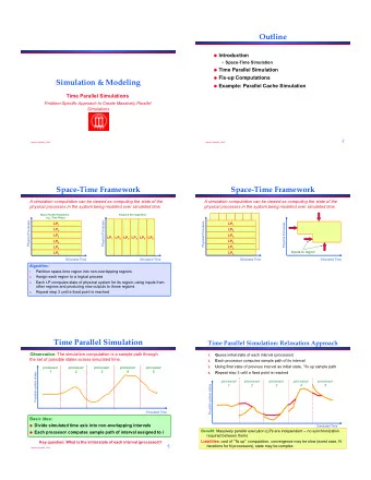
Outline • Combinational & sequential logic • Single-cycle CPU • Multi-cycle CPU 1
Combinational Element combinational n n input output logic •Output determined entirely by input •Contains no storage element 2
Examples of Combinational Elements M •Multiplexor selects one out of 2 n 2 n 1 U inputs X n •ALU performs arithmetic & logic operations – AND: 000 64 –OR: 001 zero –add: 010 ALU 64 result –subtract: 110 64 –set on less than: 111 –other 3 combinations unused 3 3
State (Sequential) Element write •State element has storage (i.e., memory) State Element •State defined by storage content input output storage •Output depends on input and the state •Write lead controls storage update •Clock lead determines time of update clock •Examples: main memory, registers, PC 4
Clocking Methodology •Needed to prevent simultaneous read/write to state elements •Edge-triggered methodology: state elements updated at rising clock edge State State Combinational element element logic 1 2 clock input 5
Input/Output of Elements State Combinational element logic 1 •Combinational elements take input from one state element at clock edge and output to another state element at the next clock edge, •Within a clock cycle, state elements are not updated and their stable state is available as input to combinational elements, •Output can be derived from a state element at the edge of one cycle and input into the same state at the next. 6
Register File •Register file is the structure that 64 contains the processor’s 32 registers 5 Read Read reg 1 data 1 Register 5 •Any register can be accessed for read Read reg 2 numbers 5 Registers or written by specifying the register Write reg Read 64 number Write data 64 data 2 Data • Register File’s I/O structure –3 inputs derived from current RegWrite instruction to specify register operands (2 for read and 1 for write) •Register file’s outputs are always –1 input to write data into a available on the output lines register •Register write is controlled by –2 outputs carrying contents of the RegWrite lead specified registers 7
MIPS64 Instruction Formats 6 5 5 16 opcode rs rd immediate I-Type Note the regularity of 6 5 5 5 5 6 instruction encoding. This is important for opcode rs rt rd shamt func R-Type implementing an efficient pipelined CPU. 6 26 J-Type opcode Offset added to PC 8
Common Steps in Instruction Execution • Execution of all instructions require the following steps – send PC to memory and fetch instruction stored at location specified by PC – read 0-2 registers, using fields specifying the registers in the instruction • All instructions use ALU functionality – data transfer instructions: compute address – ALU instructions: execute ALU operations – branch instructions: comparison & address compuation 9
Differences in Instruction Execution Data transfer (strictly load/store ISA) • – load: access memory for read data {ld R1, 0(R2)} – store: access memory for write data {ld 0(R2), R1} • ALU instruction – no memory access for operands – access a register for write of result {add R1,R2, R3} • Branch instruction – change PC content based on comparison {bnez R1, Loop} 10
Summary Fetch Decode Read Compute Access Write Registers Memory Registers add/sub X X X X X load X X X X X X store X X X X X conditional X X X X branch unconditional X X X branch 11
Data Path & Control path • Datapath is the signal path through which data in the CPU flows including the functional elements Elements of Datapath • – combinational elements – state (sequential) elements • Control path – the signal path from the controller to the Datapath elements – exercises timing & control over Datapath elements 12
What Should be in the Datapath • At a minimum we need combinational and sequential logic elements in the datapath to support the following functions – fetch instructions and data from memory – Read registers – decode instructions and dispatch them to the execution unit – execute arithmetic & logic operations – update state elements (registers and memory) 13
Datapath Schematic Registers Data Instruction Register # Memory ALU PC Address ALU Address Register # Instruction Data Register # Memory Data What is this for? 14
Datapath Building Blocks: Instruction Access • Program Counter (PC) How wide is this in MIPS64? a register that points to the next – instruction to be fetched – it is incremented each clock cycle • Content of PC is input to Instruction Memory ALU Adder • The instruction is fetched and supplied to upstream datapath elements 4 Adder is used to increment PC by 4 in • preparation for the next instruction (why 4?) Read PC • Adder: an ALU with control input address hardwired to perform add instruction Instruction only 32 • For reasons that will become clear later, we assume separate memory Instruction units for instructions & data Memory 15
Datapath Building Blocks: R-Type Instruction 6 5 5 5 5 6 ALUop opcode rs rt rd shamt func Read 5 R-Type Format Read reg 1 data 1 Instruction 5 zero Read reg 2 ALU Register ALU 5 Used for arithmetic & logic • Write reg File operations Read Write data data 2 • Read two register, rs and rt • ALU operates on registers’ content RegWrite • Write result to register rd • Example: add R1, R2, R3 – rs=R2, rt=R3, rd=R1 • Controls – RegWrite is asserted to enable write at clock edge – ALUop to control operation 16
I-Type Instruction: load/store • rs contains the base field for the displacement address mode • rt specifies register 6 5 5 16 to load from memory for – opcode rs rt immediate I-Type load – to write to memory for store • Immediate contains address LW R2, 232(R1) offset SW R5, -88(R4) To compute memory • address, we must – sign-extend the 16-bit immediate to 64 bits add it to the base in rs – 17
Required Datapath Elements for load/store • Register file – load : registers to read for base address & to write for data store : registers to read for base address & for data – Sign extender • – to sign-extend and condition immediate field for 2’s complement addition of address offset using 64-bit ALU • ALU 16 64 sign – to add base address and sign-extended immediate field extend • Data memory to load/store data: – memory address; data input for store; data output for load – control inputs: MemRead, MemWrite, clock 18
Datapath Building Blocks: load/store 6 5 5 16 opcode rs rt immediate I-Type ALUop MemWrite Read 5 Read reg 1 zero data 1 Instruction 5 Read reg 2 ALU Read ALU 5 Registers Address Write reg data Read Data Write data data 2 Memory Write data RegWrite 16 sign 64 MemRead extend 19
I-Type Instruction: bne Branch datapath must compute • branch condition & branch address rs and rt refer to registers to be • compared for branch condition 6 5 5 16 if Reg[rs] != Reg[rd], • opcode rs rt immediate I-Type PC = PC + Imm<< 2 (note that at – this point PC is already incremented. In effect PC current =(PC previous +4) + Imm<< 2 bne R1, R2, Imm • else if Reg[rs] == Reg[rt] – PC remains unchanged: PC current =(PC previous +4) – the next sequential instruction is taken 64 shift 64 • Required functional elements left 2 – RegFile, sign extender, adder, shifter 20
Sign Extend & Shift Operations • Sign extension is required because – 16-bit offset must be expanded to 64 bits in order -20189 -20189 -80756 to be used in the 64-bit adder 0xb123 0xffffb123 0xfffec48c we are using 2’s – complement arithmetic 1 sign 64 shift 64 6 • Shift by 2 is required extend left 2 because ALU Adder instructions are 32-bits wide – and are aligned on a word (4 bytes) boundary PC+4 – in effect we are using an 18- bit offset instead of 16 21
Datapath Building Blocks: bne 6 5 5 16 opcode rs rt immediate I-Type ALUop = subtract Read 5 Read reg 1 To branch data 1 zero Instruction 5 Read reg 2 control logic ALU ALU Registers Write reg Read Write data data 2 RegWrite 16 sign 64 shift extend left 2 Branch target ALU Adder PC+4 from Instruction Datapath 22
Computing Address & Branch Condition • The register operands of bne are compared in the same ALU we use for load/store/arithmetic/logic instructions – the ALU provides a ZERO output signal to indicate condition – the ZERO signal controls what instruction will be fetched next depending on whether the branch is taken or not • We also need to compute the address – we may not be able to use the ALU if it is being used to compute the branch condition (more on this later) – need an additional ADDER (an ALU hardwired to add only) to compute branch address 23
Recommend
More recommend
Explore More Topics
Stay informed with curated content and fresh updates.

