Outline Objective of Presentation Objective of Presentation Digital - PowerPoint PPT Presentation
Outline Objective of Presentation Objective of Presentation Digital IC Project and Verification Synthesis Basic synthesis flow i h i fl ASIC Synthesis DesignCompiler Synthesis script Deepak Dasalukunte & Joachim
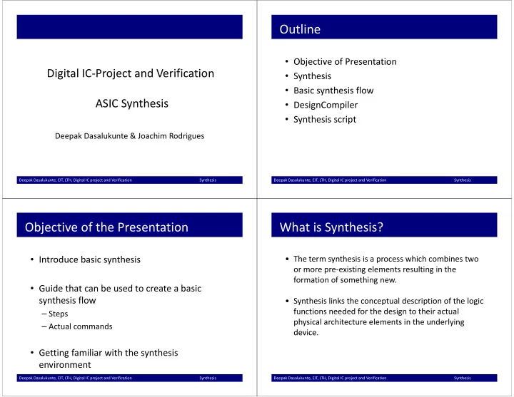
Outline • Objective of Presentation Objective of Presentation Digital IC ‐ Project and Verification • Synthesis • Basic synthesis flow i h i fl ASIC Synthesis • DesignCompiler • Synthesis script Deepak Dasalukunte & Joachim Rodrigues Deepak Dasalukunte & Joachim Rodrigues Deepak Dasalukunte, EIT, LTH, Digital IC project and Verification Synthesis Deepak Dasalukunte, EIT, LTH, Digital IC project and Verification Synthesis Objective of the Presentation What is Synthesis? • Introduce basic synthesis Introduce basic synthesis • The term synthesis is a process which combines two The term synthesis is a process which combines two or more pre ‐ existing elements resulting in the formation of something new. • Guide that can be used to create a basic G id h b d b i synthesis flow • Synthesis links the conceptual description of the logic f functions needed for the design to their actual ti d d f th d i t th i t l – Steps physical architecture elements in the underlying – Actual commands device. device • Getting familiar with the synthesis g y environment Deepak Dasalukunte, EIT, LTH, Digital IC project and Verification Synthesis Deepak Dasalukunte, EIT, LTH, Digital IC project and Verification Synthesis
What is Synthesis? Synthesis Tool ‐ Design Compiler (DC) An idea is incorpareted Functional description FSM FSM (text, graphic) into a manufacturable • Common tool provided by Synopsys device by doing • Well known in industry and academia • Well ‐ known in industry and academia synthesis: s nthesis Al Algorithms and i h d Behavioral Model architectures in HDL HDL – Translation • Online support: https://solvnet.synopsys.com/ – Logic Optimization – Logic Optimization • Command help in Synopsys ‐ DC GUI. Complete design with clock RTL – Gate mapping Architectural HDL and registers • Graphical mode p • Shell mode Gate ‐ level Place and Synthesis Netlist Route Deepak Dasalukunte, EIT, LTH, Digital IC project and Verification Synthesis Deepak Dasalukunte, EIT, LTH, Digital IC project and Verification Synthesis Synthesis Flow Libraries • Vendor delivers technology libraries as ASCII file Read Design ( .lib_) (* lib ) Prepare Prepare – describes parameters and rules for a particular Specify technology(130nm,90nm, 65nm...). Clock • Every process consists of logic cells that has Specify different functionality. Constraints – full adder, multiplier, flip ‐ flop, XOR, NAND etc Synthesis • Compiled for Synopsys DC usage (*.db) • Various libraries, e.g., low ‐ leakage (LL) or high ‐ Check Synthesis speed (HS) are usually available . Create Netlist Deepak Dasalukunte, EIT, LTH, Digital IC project and Verification Synthesis Deepak Dasalukunte, EIT, LTH, Digital IC project and Verification Synthesis
Libraries Synthesis Flow Read Design • Target library is used by DC to build the circuit g y y (Prepare ) (Prepare ) • DC chooses gates from libraries • Gate timing information is included in libraries • Defined in .synopsys_dc.setup – Copied into the working directory when init scripts are run. – specifies the libraries being used and other configurations. specifies the libraries being used and other configurations • *.lib information for the memory needs to be read by DC. – SYNTAX: read_lib memoryX.lib – SYNTAX: write_lib memoryX (writes the memory in .db format) • If *.db is already available, include them in the link_library and target library target_library Deepak Dasalukunte, EIT, LTH, Digital IC project and Verification Synthesis Deepak Dasalukunte, EIT, LTH, Digital IC project and Verification Synthesis Read Design Syntax: Analyze analyze • DC reads both RTL designs and gate ‐ level netlist. DC reads both RTL designs and gate level netlist. [ library library_name ] [ -library library name ] [ -format vhdl | verilog | sverilog ] file_list • DC reads design files with analyze and elaborate DC reads design files with analyze and elaborate - library library_name commands Maps the work library to library_name . – analyze : analyzes HDL files and stores the intermediate y y By default, analyze stores all output in the work library. -format vhdl | verilog | sverilog format for the HDL description in the specified library Specifies the format of the files that are to be analyzed; – elaborate: Builds a design from the intermediate format, a file_list file list VHDL VHDL entity and architecture tit d hit t Specifies a list of files to be analyzed. When specifying more than one file, • Every instance becomes unique. enclose the files in braces: { }. Example: Example: analyze -format vhdl -lib WORK {../vhdl/your_design.vhd} Deepak Dasalukunte, EIT, LTH, Digital IC project and Verification Synthesis Deepak Dasalukunte, EIT, LTH, Digital IC project and Verification Synthesis
Syntax: Elaborate Synthesis Flow elaborate design_name Read Design Prepare Prepare [- library library_name | -work library_name ] [- library library name | -work library name ] [- architecture arch_name ] Specify [- update ] Clock design_name Specifies the name of the design to be built. This design can be a Verilog module, a VHDL entity or a VHDL configuration VHDL entity, or a VHDL configuration. -library library_name Specifies the library name that work is to be mapped to. By default, elaborate looks in the work library for the design to be built. y g -architecture arch_name Specifies the name of the architecture, .e.g., behavioral, structural, rhubarb, … Example: Example: elaborate fir –lib WORK –arch structural Deepak Dasalukunte, EIT, LTH, Digital IC project and Verification Synthesis Deepak Dasalukunte, EIT, LTH, Digital IC project and Verification Synthesis Clock Definition Syntax: create_clock create_clock In DC clock is ideal no In DC, clock is ideal: no [ -period period_value ] [ -name clock_name ] buffers, no DRC, no [ source_objects ] optimization p -period period_value The period of the clock waveform in library time units. • Required Definitions default unit is ns default unit is ns ‐ A clock constrains timing A l k t i ti i – Clock period -name clock_name paths bewteen registers. Specifies the name of the clock being created. – Clock name source objects _ j ‐ A design may have A design may have – Clock source Cl k Specifies a list of pins or ports on which to apply this clock. several clocks. – (Duty cycle (50% default)) – (Offset/skew) (Offset/skew) Real clock synthesis takes Real clock synthesis takes Example: create_clock clk –period 20 -name clk place in PnR Deepak Dasalukunte, EIT, LTH, Digital IC project and Verification Synthesis Deepak Dasalukunte, EIT, LTH, Digital IC project and Verification Synthesis
Clock Skew Synthesis Flow Read Design Worst case clock skew needs to be defined Worst case clock skew needs to be defined Prepare Prepare – technology and design dependent Specify – not easy to determine Clock – Around 2% of clock period Specify Constraints Syntax: set_clock_uncertainty 1 name_of_your_clock also set_fix_hold name_of_your_clock Deepak Dasalukunte, EIT, LTH, Digital IC project and Verification Synthesis Deepak Dasalukunte, EIT, LTH, Digital IC project and Verification Synthesis Synthesis Constraints Constraining Input Paths High ‐ speed or Low ‐ area? t p f max =1/t pmax slow slow Logic is triggered by same clock Need to Specify propagation delay of external logic that y g fast fast drives your logic AREA large small User ‐ controlled constrainst define the goal Deepak Dasalukunte, EIT, LTH, Digital IC project and Verification Synthesis Deepak Dasalukunte, EIT, LTH, Digital IC project and Verification Synthesis
Constraining Input Paths Constraining Output Paths Need to Specify propagation delay of external logic Need to Specify propagation delay of external logic that is driven by your logic SYNTAX set_input_delay –max 5.6 –clock clk [get_ports A] set_output_delay –max 4 –clock clk [get_ports B] This command could be useful in the project part if you need to connect several dersigns. Not needed for assignment 3/4. Deepak Dasalukunte, EIT, LTH, Digital IC project and Verification Synthesis Deepak Dasalukunte, EIT, LTH, Digital IC project and Verification Synthesis Constraining Area Area vs. speed Area is expensive and needs to be constrained • For a high ‐ speed circuit do not set any area For a high speed circuit do not set any area set_max_area constraint and specify a high clock frequency. sets the max_area attribute to a specified value on the current design. The max area attribute represents the target area of the design and is used _ p g g • For an area optimized circuit set area to 0 and • For an area optimized circuit set area to 0 and by the compile command to calculate area cost of the design. specify a low clock frequency. SYNTAX set_max_area area_value • Two synthesis runs are necessary. T h i l – Highest speed set_max_area 0 e.g. – Smallest area. • Synthesis tool prioritizes total negative slack over area . • A design that does not met timing will not work. • Compile does not create new delay violations or worsen existing delay Compile does not create new delay violations or worsen existing delay violations on a path that has negative delay slack in order to improve area. Deepak Dasalukunte, EIT, LTH, Digital IC project and Verification Synthesis Deepak Dasalukunte, EIT, LTH, Digital IC project and Verification Synthesis
Recommend
More recommend
Explore More Topics
Stay informed with curated content and fresh updates.


