MOSFET Characteristics at Cryogenic Temperatures Juan Avalos - PowerPoint PPT Presentation
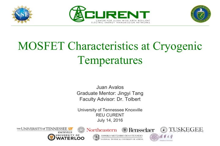
MOSFET Characteristics at Cryogenic Temperatures Juan Avalos Graduate Mentor: Jingyi Tang Faculty Advisor: Dr. Tolbert University of Tennessee Knoxville REU CURENT July 14, 2016 Objective: Determine the semiconductor devices with the
MOSFET Characteristics at Cryogenic Temperatures Juan Avalos Graduate Mentor: Jingyi Tang Faculty Advisor: Dr. Tolbert University of Tennessee Knoxville REU CURENT July 14, 2016
Objective: Determine the semiconductor devices with the least energy losses to use in the DC-AC inverter for Boeing & NASA aircraft. Devices: Microsemi, Infineon, IXYS Characteristics: On-state resistance Body Diode Switching Losses Breakdown Voltage 2
On-State Resistance (R DS-ON )& Body Diode Schematic • Same schematic, different settings • R DS-ON gate input=10V • Body diode gate input=0V • Polarity changes opposite current paths
On-State Resistance Results (Infineon) Curve Tracer Results 1.20E+02 • Curve Tracer plots are 1.00E+02 used to calculate the on-state resistance. 8.00E+01 Drain Current (A) • Use rated current and 25 C 0 C corresponding voltage 6.00E+01 -30 C -60 C -90 C -120 C 4.00E+01 -150 C -180 C 2.00E+01 0.00E+00 0.00E+00 5.00E+00 1.00E+01 1.50E+01 2.00E+01 Drain Source Voltage (V) 4
On-State Resistance Cont. Temperature Effect 0.18 • Calculated on-state resistance using previous 0.16 plot at different On-State Resistance (Ω) 0.14 temperatures. 0.12 • R DS-ON = V DS /I RATED 0.1 0.08 0.06 0.04 0.02 0 -2.00E+02-1.50E+02-1.00E+02-5.00E+01 0.00E+00 5.00E+01 Temperature (C)
Body Diode • Device in cut off region • Polarity of input is reversed w/ respect to on-state resistance • Reverse drain current shorts the source and drain • High current path created through body diode
Results of Body Diode (Infineon) 100 90 80 70 60 Id(A) 50 40 30 20 10 0 0 0.5 1 1.5 2 2.5 Vsd(V)
Switching Losses Schematic Cryo. Chamber + – DC Upper Load source Diode Inductor DC Link Capacitor Scope AUX Power Power Supply Supply Signal Gate Lower Signal Isolator/ Driver Switch Generator Logic
Switching Losses Cont. • Double Pulse Test: First pulse is used to charge up • inductor current at desired value. First Falling edge = turn-off • switching transient Second Rising edge = turn-on • switching transient • Parasitic inductance & capacitance • Cause ringing and overshoot in switching transients losses
Switching Energy Losses Curve (Infineon) 30 20A 20A 25 20 Esw(uJ) 10A 10A 15 3A 3A 10 5 0 0 50 100 150 200 250 300 350 Temperature(K)
Breakdown Voltage Ampere meter • High voltage applied; near the rated A voltage of the device • Current = 1mA is considered Cryo. chamber breakdown for the device. D Device + • Gate and source shorted High voltage • 100 kOhms resistor under – DC source G test (DUT) S Current limiting resistor
750 Breakdown Voltage 700 Results Breakdown Voltage(V) 650 • The Drain-Source Voltage • Determined by reverse breakdown behavior 600 • Reduces as temperature decreases 550 500 450 70 120 170 220 270 320 Temperature(K)
Conclusion Efficiency of MOSFET devices improves at cryogenic operation: • Faster switching w/ less losses • Allows larger current with less overshooting • On-state resistance drastically decreases
Acknowledgements This work was supported primarily by the ERC Program of the National Science Foundation and DOE under NSF Award Number EEC-1041877. Other US government and industrial sponsors of CURENT research are also gratefully acknowledged. 14
Questions and Answers 15
Recommend
More recommend
Explore More Topics
Stay informed with curated content and fresh updates.
