Challenges for Future Cryogenic Electronics Challenges for Future - PowerPoint PPT Presentation
Challenges for Future Cryogenic Electronics Challenges for Future Cryogenic Electronics Shaorui Li, Gianluigi De Geronimo, Jie Ma, Hucheng Chen, Jack Fried, Alessio DAndragora, and Veljko Radeka Brookhaven National Laboratory, NY, USA Outline:
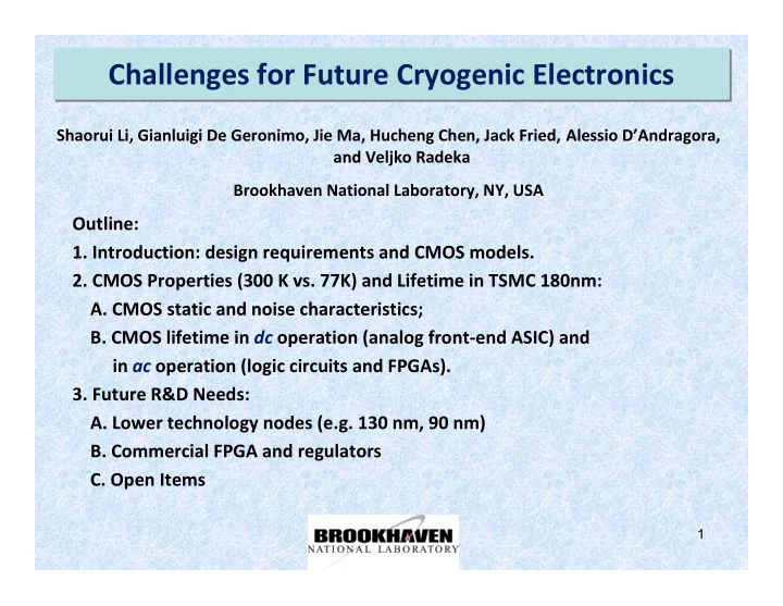
Challenges for Future Cryogenic Electronics Challenges for Future Cryogenic Electronics Shaorui Li, Gianluigi De Geronimo, Jie Ma, Hucheng Chen, Jack Fried, Alessio D’Andragora, and Veljko Radeka Brookhaven National Laboratory, NY, USA Outline: 1. Introduction: design requirements and CMOS models. 2. CMOS Properties (300 K vs. 77K) and Lifetime in TSMC 180nm: A. CMOS static and noise characteristics; B. CMOS lifetime in dc operation (analog front ‐ end ASIC) and in ac operation (logic circuits and FPGAs). 3. Future R&D Needs: A. Lower technology nodes (e.g. 130 nm, 90 nm) B. Commercial FPGA and regulators C. Open Items 1
Introduction Introduction • The design of front ‐ end CMOS ASICs operating in cryogenic (~ ‐ 200 C) environment poses some challenges. The stringent requirements include: low ‐ noise, low ‐ power, precise signal processing, and long lifetime (>20~30 years). Models: • CMOS vendors focus their models on temperature ranges from ‐ 40 C to 125 C and on device lifetimes of about 10 years. • The design of cryogenic front ‐ end ASICs for HEP requires models capable of accurately reproducing static and dynamic response, noise performance, lifetime of CMOS devices and circuits operating in the ~ 80K range. •These models must extend to the moderate inversion region, considering the low ‐ power requirements on analog circuits. 2
Static Characteristics: Larger Sub-Threshold Slope at 77 K Static Characteristics: Larger Sub-Threshold Slope at 77 K 10 10 CMOS018 MEASURED CMOS018 SIMULATED (foundry parameters) I D vs V DS LN LN RT RT 8 8 6 6 I D [mA] I D [mA] 4 4 2 2 NMOS, L=0.18µm, W=10µm NMOS, L=0.18µm, W=10µm 0 0 0.0 0.3 0.6 0.9 1.2 1.5 1.8 0.0 0.3 0.6 0.9 1.2 1.5 1.8 V DS [V] V DS [V] 1 1 10 10 I D vs V GS CMOS018 CMOS018 g m g m 0 0 10 10 I D I D ~72mV/dec ( ln(10)nV T ) ~72mV/dec ( ln(10)nV T ) -1 -1 10 10 I D [mA], g m [mS] I D [mA], g m [mS] MEASURED SIMULATED LN (foundry parameters) -2 -2 10 10 RT LN RT -3 ~18mV/dec -3 ~18mV/dec 10 10 -4 -4 10 10 NMOS, L=0.18µm, W=10µm NMOS, L=0.18µm, W=10µm -5 -5 10 10 0.0 0.3 0.6 0.9 1.2 1.5 1.8 0.0 0.3 0.6 0.9 1.2 1.5 1.8 V GS [V] V GS [V] 3 Some differences in saturation voltage, sub-threshold slope, transconductance
Static Characteristics: Lower Power at 77K Static Characteristics: Lower Power at 77K MEASURED 120 Favorable for cryogenic operation: NMOS PMOS T=77K 100 L=360nm • higher g m -> lower noise L=270nm • higher g m /I D -> lower power L=180nm 80 -1 ] g m /I D [V NMOS PMOS T=300K 60 L=360nm L=270nm 40 L=180nm 20 CMOS018 0 -6 -5 -4 -3 -2 -1 0 1 2 10 10 10 10 10 10 10 10 10 Drain Current Density [mA/mm] Design region (approx.) Asymptotic value at weak inversion: for low power and low noise at 77K (moderate ~ 30 at T 300 K g q m inversion): gm increase I nk T ~ 116 at T 77 K D B by a factor of ~2. 4
Noise: Lower White Noise and Lower PMOS 1/f Noise at 77K Noise: Lower White Noise and Lower PMOS 1/f Noise at 77K T = 300K T = 77K 3 3 10 10 L=180nm, W=1mm (20µm x 50) L=180nm, W=1mm (20µm x 50) Input noise spectral density [nV/ Hz] Input noise spectral density [nV/ Hz] V DS =400mV, T=300K V DS =400mV, T=77K 2 2 10 10 1/f 1/f NMOS NMOS I D =3.2mA (IC=3) I D =3.2mA (IC=1) 1 1 10 10 PMOS PMOS I D =0.7mA (IC=1) I D =0.7mA (IC=0.3) fit curve fit curve 0 0 10 10 white white 1/f 1/f CMOS018 CMOS018 -1 -1 10 10 1 2 3 4 5 6 7 8 1 2 3 4 5 6 7 8 10 10 10 10 10 10 10 10 10 10 10 10 10 10 10 10 Frequency [Hz] Frequency [Hz] • lower white noise than at 300K • comparable 1/f noise amplitude • NMOS (i.e. comparable noise at 1 Hz) • comparable 1/f noise amplitude • different 1/f noise slope: • Lorentzian packet PMOS > NMOS • PMOS ‐ > PMOS more advantageous for 5 • lower 1/f noise amplitude low ‐ noise application. • 1/f noise slope < 1
Input MOSFET Optimization for LAr TPC Analog Front-End ASIC Input MOSFET Optimization for LAr TPC Analog Front-End ASIC 1200 N036 1100 Design input PMOSFET 1000 P018 for 200pF detector 900 ENC [rms electrons] P027 electrodes (wires)! 800 P018 700 P036 300K 600 77K P027sim 500 C DET =200pF PK =1 s P027 400 I D =2mA 300 10 1 100 1000 Gate Width [mm] An improvement of ENC Selected size and operating point: (~530 e ‐ to ~420 e ‐ ) achieved original (simul. noise) vs. revised (meas. noise) • I D = 2 mA (3.6 mW) using measured noise • W/L = 10 mm / 270 nm 20 mm / 270 nm parameters. 0.3 1 • IC 300K ≈ 0.4 IC 77K = 1.25 48 mS 118mS • g m_300K ≈ 45 mS g m_77K = 90 mS 6 • C g_300K ≈ 14 pF 25 pF 28 pF C g_77K = 18 pF
CMOS Lifetime at Cryogenic Temperatures CMOS Lifetime at Cryogenic Temperatures Introduction • Most failure mechanisms (e.g. electromigration, stress migration, time ‐ dependent dielectric breakdown, and thermal cycling) are strongly temperature dependent and become negligible at cryogenic temperature. The only remaining mechanism that may affect the lifetime of CMOS devices at cryogenic temperature is the degradation (aging) due to channel hot carrier effects (HCE). • The degradation mainly concerns NMOS devices ‐ PMOS usually exhibits a lifetime two orders of magnitude longer than NMOS. • Lifetime due to aging : A limit defined by a chosen level of monotonic degradation in e.g., drain current, transconductance, due to a well understood mechanism. The device “fails” if a chosen parameter gets out of the specified circuit design range. This aging mechanism does not result in sudden device failure. • Our study and experiments suggest that the lifetime due to HCE at cryogenic temperature, as at room temperature, is limited by a predictable and a very gradual degradation (aging) mechanism which can be controlled by the electronic design . In this study we have been following the basics established in the literature, e.g., Hu et al. (1985), and the practices adopted more recently by Chen&Cressler et al. (2006), as well as by industry. 7
HCE: Basic Mechanism HCE: Basic Mechanism • Degradation is due to impact ionization: interface state generation & charge trap in oxide → shift in V th and g m • Substrate current is a monitor of impact ionization • increases with drain voltage • is higher in short channel devices • has a maximum at V GS ≈ V DS /2 • Commercial technologies are rated > 10 years lifetime (10% g m shift) at T = 300 K, L = L min , V DS = nominal V DD +5%, V GS ≈ V DS /2) • A lower temperature results in increased mean free path λ increasing the substrate current I sub and g m degradation. Degradation is independent of temperature if the product λ (V DS – V SAT ) is kept constant. • Accelerated lifetime test (well ‐ established by foundries): transistor is placed under a severe electric filed stress (large V DS ), to reduce the lifetime due to hot ‐ electron degradation to a practically observable range, by a drain source voltage considerably higher than the nominal voltage (1.8V for L min =180nm). 8
CMOS in dc Operation: Analog Front-End ASIC CMOS in dc Operation: Analog Front-End ASIC Measurement Type I: “Stress Plot” I 1 ln ds it W q E V V 3 m ds dsat 10 1.7V 1 1.8V I W 1E9 ds a I I Lifetime ~ 3200 yrs at Vds=1.8V, 77K sub ds Vds=2.8V 1E7 2 10 300K Slope ~3.10 300K 100000 *Ids/W [s*A/ m] *I DS /W (s*A/ m) Vds=3.0V 77K 1000 1 ASIC design: 10 Vds=3.1V Vds<1.5V Vds=2.8V 10 Vds=3.2V 0.1 0 Vds=3.0V 10 77K Slope ~2.94 1E-3 Vds<1.8V 3.2, 3.1, 3.0, 2.8 V Vds=3.2V -1 1E-5 10 -2 -1 0 0.1 0.2 0.3 0.4 0.5 0.6 10 10 10 -1 ) 1/V DS (V Isub/Id • The measured points at both 300K and 77K are very close to the characteristic a 3 slope for the interface state generation, it i • The projected lifetime at 300K is ~ an order of magnitude longer than at 77K. Reducing V ds at 77K by ~ 6% makes the lifetime equal to that at 300K. Design at low I ds /W for even longer lifetime. 9
Recommend
More recommend
Explore More Topics
Stay informed with curated content and fresh updates.
