Module 12 Latch as a Comparator References - Prof. Boris Murmanns - PowerPoint PPT Presentation
11 11 Module 12 Latch as a Comparator References - Prof. Boris Murmanns slides from VLSI Data Conversion Circuits, Stanford University, 2013. - Section Latched Comparators onwards from chapter Comparators, Analog
11 11 Module 12 Latch as a Comparator References - Prof. Boris Murmann’s slides from “VLSI Data Conversion Circuits”, Stanford University, 2013. - Section “Latched Comparators” onwards from chapter “Comparators”, Analog Integrated Circuit Design by T. C. Carusone, D. A. Johns and K. Martin, J. Wiley & Sons, 2012. - “Clocked Comparator” from chapter “Submicron CMOS Circuit Design”, CMOS Mixed-signal Circuit Design by R. Jacob Baker, Wiley India, IEEE press, reprint 2009. - “Comparator” from chapter “Nonlinear Analog Circuits”, CMOS Circuit Design, Layout and Simulation by R. Jacob Baker, Wiley India, IEEE press, 2008. - “The StrongArm Latch”, B. Razavi, IEEE Solid-State Circuits Magazine, Spring 2015. IIT-Bombay Lecture 11 M. Shojaei Baghini
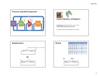
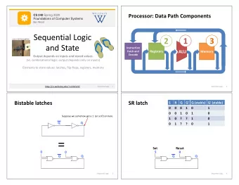
12 12 Replacing Cascade of N Integrators with a V DD Closed Loop of Integrators ! 2 Latch (regenerative ! 1 ! 1 sense amplifier) V IP V IN C L ! 2 C L V SS • Each inverter is a G m module driving a capacitive load and hence behaves as an integrator. • A closed loop of two inverters is mimicking cascade of infinite number of integrators. IIT-Bombay Lecture 11 M. Shojaei Baghini
13 13 Latch as a Comparator " # ! = $ % !! Latch gain B. Murmann’s course, Stanford Univ., 2013 IIT-Bombay Lecture 11 M. Shojaei Baghini
14 14 Latch as a Comparator - Example B. Murmann’s course, Stanford Univ., 2013 IIT-Bombay Lecture 11 M. Shojaei Baghini
15 15 Linear Behavior of log(V diff (t)) versus t and Initial Condition B. Murmann’s course, Stanford Univ., 2013 IIT-Bombay Lecture 11 M. Shojaei Baghini
16 16 Analysis of Latch Delay " #$,&#'() T d,latch = ! latch ln " #$,* C ≈ a × WLC ox , 1<a<2 g m ≈ b × + C ox W/L × V GST , 0.5<b<1 (either NMOS or PMOS transistor) ⇒ ! latch ≈ d × L 2 /( + n × V GST ) where 1<d<4 Velocity saturation: ! latch ≈ a × L/v sat K. Martin’s book, 2012 • B. Murmann’s course, Stanford • Univ., 2013 IIT-Bombay Lecture 11 M. Shojaei Baghini
17 17 End of Lecture 11 IIT-Bombay Lecture 11 M. Shojaei Baghini
Mixed-Signal VLSI Design Course Code: EE719 Department: Electrical Engineering Lecture 13: February 10, 2020 Instructor Name: M. Shojaei Baghini E-Mail ID: mshojaei@ee.iitb.ac.in 1
2 2 Module 13 Effect of Offset in Latched Comparator Reference An Analysis of Latch Comparator Offset Due to Load • Capacitor Mismatch, A. Nikoozadeh and B. Murmann, IEEE TCAS-II , Dec. 2006 IIT-Bombay Lecture 13 M. Shojaei Baghini
3 3 Shortcomings Associated with the Stand- alone Latch as a Comparator Static and dynamic offset of latch • Charge injection from switches • Kickback noise • Low CMRR • IIT-Bombay Lecture 13 M. Shojaei Baghini
4 4 Latch Offset 1 + ∆) 1 + ∆. / ! "#0 = − 1 ! "+0 − ! #,+ + ΔV sw ) . / 1 + ∆) ! "#0 = ) − 1 ! "+0 − ! #,+ + ΔV sw V ON0 : Initial voltage , C LP =C , C LN =C+ΔC Example: 5% mismatch, V ON0 = 300mV, V SWN = 0.9V , ΔV sw = 20mV ⇒ Initial offset voltage V OS0 = 35mV! Inspired from: An Analysis of Latch Comparator Offset Due to Load Capacitor Mismatch, A. Nikoozadeh and B. Murmann, IEEE TCAS-II , Dec. 2006 IIT-Bombay Lecture 13 M. Shojaei Baghini
5 5 Pre-amplifier Followed by Latch 1 + ∆) ! "#0 = ) − 1 ! "+0 − ! #,+ + ΔV sw V ON0 : Initial voltage , C LP =C , C LN =C+ΔC Example: 5% mismatch, V ON0 = 300mV, V SWN = 0.9V , ΔV sw = 20mV ⇒ Initial offset voltage V OS0 = 35mV! Assume pre-amp gain = 8 ⇒ Equivalent offset a the input of pre- amp = 35/8 ≈ 4.4 mV. Even considering offset of 2mV for the pre-amp the total equivalent input offset voltage ≈ 4.8 mV IIT-Bombay Lecture 13 M. Shojaei Baghini
Recommend
More recommend
Explore More Topics
Stay informed with curated content and fresh updates.


