Digital Design Discussion: Flip-Flops D-Latch Design Latch vs. - PowerPoint PPT Presentation
Principles Of Digital Design Discussion: Flip-Flops D-Latch Design Latch vs. Flip-Flop Timing D-latch Design Design a gated D-latch using NAND gates and inverters. Draw the schematic and create a truth table for it. An implementation of
Principles Of Digital Design Discussion: Flip-Flops D-Latch Design Latch vs. Flip-Flop Timing
D-latch Design Design a gated D-latch using NAND gates and inverters. Draw the schematic and create a truth table for it. An implementation of simple gates is provided for reference. Procedure D 2.0 Q 1. Convert NOR and AND to NAND C Q’ 2.0 Logic schematic 2. Redraw schematic and create truth table D D C D Q Q(next) 2.0 2.0 Q Q 0 X 0 0 0 X 1 1 C C 1 0 X 0 Q’ Q’ 2.0 2.0 1 1 X 1 Truth table Logic schematic Logic schematic 2 DIGITAL DESIGN 101, University of California Flip-Flops
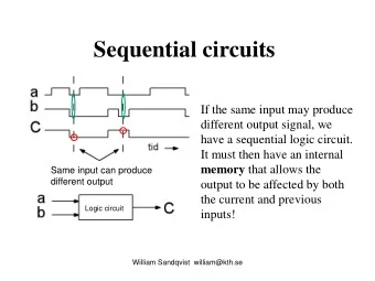
Latch and Flip-Flop Comparison Compare the behavior of D latch and D flip-flop devices by completing the timing diagram in the figure below. Assume each device initially stores a 0. Latches are level-sensitive since they respond to input changes during clock width. (e.g. when clock is 1) Flip-Flops respond to input changes only during the change in clock signal, (e.g. at rising edge of clock signal) C D Q(D latch) Q(D flip-flop) 3 DIGITAL DESIGN 101, University of California Flip-Flops
Latch and Flip-Flop Comparison Compare the behavior of D latch and D flip-flop devices by completing the timing diagram in the figure below. Assume each device initially stores a 0. Latches are level-sensitive since they respond to input changes during clock width. (e.g. when clock is 1) Flip-Flops respond to input changes only during the change in clock signal, (e.g. at rising edge of clock signal) C D Q(D latch) Q(D flip-flop) 4 DIGITAL DESIGN 101, University of California Flip-Flops
Recommend
More recommend
Explore More Topics
Stay informed with curated content and fresh updates.


