Microdisk Cavity FDTD Simulation on FPGA using OpenCL Tobias - PowerPoint PPT Presentation
Microdisk Cavity FDTD Simulation on FPGA using OpenCL Tobias Kenter, Christian Plessl Paderborn Center for Parallel Computing and Department of Computer Science Paderborn University 1 Microdisk Cavity Microdisk cavity in perfect
Microdisk Cavity FDTD Simulation on FPGA using OpenCL Tobias Kenter, Christian Plessl Paderborn Center for Parallel Computing and Department of Computer Science Paderborn University 1
Microdisk Cavity • Microdisk cavity in perfect metallic environment – Well studied nanophotonic device – Point-like time-dependent source (optical dipole) – Known analytic solution (whispering gallery modes) 0.18 source 0.16 0.14 0.12 0.1 vacuum 0.08 0.06 0.04 perfect metal 0.02 0 experimental setup: microdisk cavity result: energy density • Simulations can help to investigate other nanophotonic setups 2
Computational Nanophotonics • Physics: Maxwell's partial differential equations – Electric field E – Magnetic field H – Material constants (electric permittivity ε, magnetic permeability μ) • Simulation: FDTD stencils – Stencil for dielectric material in 2D updateE(*ex, *ey, *hz) { ex[x,y] = ca * ex[x,y] + cb * (hz[x,y] - hz[x,y-1]); ey[x,y] = ca * ey[x,y] + cb * (hz[x-1,y] - hz[x,y]); } updateH(*ex, *ey, *hz) { hz[x,y] = da * hz[x,y] + db * (ex[x,y+1] – ex[x,y] + ey[x,y] – ey[x+1,y]); } 3
FPGA Pipeline for FDTD • Inside time step – Regular + parallel update operations Ø Can form customized loop pipeline on FPGA – Locality + predictable memory access updateE Ø Can prefetch and stream data • E and H are must be updated alternately (leap-frog) – Reusing local results is key to performance – Unrolling several time steps increases computational intensity updateH MEM updateE updateE updateE MEM MEM updateH updateH updateH overlap updating of update fields 2-fold unrolled, overlap fields for single iteration sequentially processing for 2 iterations 4
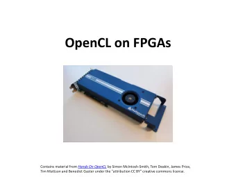
OpenCL for FPGAs • OpenCL – Covers parallelism and awareness of memory locations – Base of familiar developers (mostly GPU) – Suitable to generate competitive FDTD design on FPGA? • OpenCL-based SDAccel tool flow – OpenCL source-to-source transformation – Vivado HLS step – Vivado synthesis place + route – SDAccel Version 2016.1 • Target system – ADM-PCIE-7V3 board with Xilinx Virtex-7 XC7VX690T + 2x 8GB DDR3 memory 5
Design Steps 1. Wrap main loop into OpenCL kernel – First FPGA design up and running after few hours – ~1000x slower than CPU 2. Generate FPGA pipeline for E and H updates – Burst transfers to local memory – Compute from local memory – Pipeline main loop with low initiation interval 3. On the way… – Separate compute + transfer kernels, coupled through pipes – Code transformations in compute kernel 4. Unroll as many time steps as resources permit – Allow data reuse – Instantiate many individual buffers 6
OpenCL-based FPGA Design Read E_x E_y H_z ... Burst Local trans- Memory fers (BRAM) P i p e more Pipes Compute Kernel Global Stage 1 Memory (DDR3 on Local Memory ... ... ... ADM- Stage 2 PCIE-7V3 board) Local Memory ... ... ... ... Stage 36 Pipe more Pipes Write E_x ... Burst E_y H_z trans- fers 7
Results • 36 pipeline stages, initiation interval 2 • 140MHz (down from original target 200MHz) SDAccel, ADM-PCIE-7V3, 36 Pipeline Stages 2500 Maxeler, MAX3424A, 15 Pipeline Stages [1] OpenMP, 2x Xeon E5620, 8 Threads [2] 2000 Mcells/s 1500 1000 500 0 2 16 2 18 2 20 2 22 2 24 Grid points 8
Conclusion • Resulting design with OpenCL is very competitive • Code is adapted to FPGA target and current tool capabilities – Much lenghty boilerplate may go away with maturing tools and better understanding of them – Performance portability not explored (currently design with singe work-item) 9
Thank you! 10
Recommend
More recommend
Explore More Topics
Stay informed with curated content and fresh updates.
