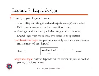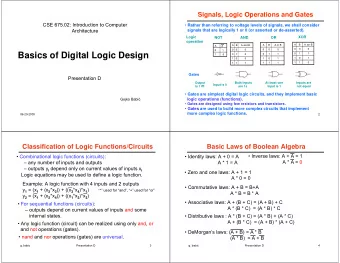
Logic Synthesis Page 1 Introduction to Digital VLSI Logic - PowerPoint PPT Presentation
Introduction to Digital VLSI Logic Synthesis Logic Synthesis Page 1 Introduction to Digital VLSI Logic Synthesis Course Outline Design Compiler Overview Some Words about Physical Compiler Coding Styles Partitioning
Introduction to Digital VLSI Logic Synthesis Logic Synthesis Page 1
Introduction to Digital VLSI Logic Synthesis Course Outline • Design Compiler Overview • Some Words about Physical Compiler • Coding Styles • Partitioning • Design Compiler Commands • Additional Commands for Physical Compiler • Timing Analysis • Interaction with Layout Tools • Speed/Area Optimization • Logic Structure in High Level Code • Physical Compiler Overview Page 2
Introduction to Digital VLSI Logic Synthesis Design Compiler Overview Cell Libraries HDL Code (RTL) Constraints (timing and function) or mapped Gate Level (timing, area ...) (xxx.lib -> xxx.db) Design Compiler Mapped Netlist Page 3
Introduction to Digital VLSI Logic Synthesis Physical Compiler Overview Cell Libraries Physical Libraries Constraints HDL Code (RTL) (cells and technology) (timing and function) (timing & physical) or mapped Gate Level (xxx.plib -> xxx.pdb) (xxx.lib -> xxx.db) Floorplan Physical Compiler Placed Netlist Page 4
Introduction to Digital VLSI Logic Synthesis • synthesis = mapping + optimization Large Area Small Fast Slow Speed • Design Compiler is constraint-driven • Designer explores area vs. speed trade-offs simply by varying constraints Page 5
Introduction to Digital VLSI Logic Synthesis Few Synopsys rules of Thumb • “There is no ‘golden’ script for synthesis” • “The random setting of optimization switches and constraints to meet your speed goals is NOT a credible methodology” • “Physics dictates what will fit between two clock edges” Page 6
Introduction to Digital VLSI Logic Synthesis General Synopsys Synthesis Flow Analyze and Elaborate Re-code RTL RTL code Create Apply Constraints Custom Wireload Synthesis tricks Floorplan Synthesize No Constraints Identify Met? Problem Yes End Page 7
Introduction to Digital VLSI Logic Synthesis General Synopsys Physical Synthesis Flow (mpc) Analyze and Elaborate Re-code RTL RTL code Apply Constraints including sime floorplan requirements compile_physical Synthesis tricks or physopt Yes No Constraints Identify “Floorplan” Met? Problem Create Floorplan End Page 8
Introduction to Digital VLSI Logic Synthesis General Synopsys Physical Synthesis Flow (flooplan based) Resize up/down, relocate pins etc. mpc run results Analyze and Elaborate Re-code RTL RTL code Update floorplan Apply Constraints (can be based including sime on mpc run) floorplan requirements compile_physical Synthesis tricks or physopt No Constraints Identify Met? Problem Yes End Page 9
Introduction to Digital VLSI Logic Synthesis Integration with Structures and other Blocks Integrate Blocks Design Yes Rule Top-Level Compile Problems? No End • Integration may cause transition problems (violations) • Top-level compile to fix any problem • Best way is to model the structures Page 10
Introduction to Digital VLSI Logic Synthesis Coding Style • Inferring Sequential Devices • Three-State Inference • Combinational Logic • case vs. if synthesis • Finite State Machines TBD? (Exists)? Page 11
Introduction to Digital VLSI Logic Synthesis Inferring Sequential Devices • Synopsys can infer a broad range of FF’s and latches: Latch Latch Latch DFF DFF DFF Muxed MS Latch w/ w/Dual w/ DFF w/ w/Dual w/ JKFF DFF latch Async Async Sync Async Async Sync + + + + + + + + + + + • An inference report indicates type, width, and presence of: Bus, Async Reset, Async Set, Sync Reset, Sync Set and Sync Toggle. Example: Inference Report for D Flipflop with Async Reset: Register Name Type Width Bus AR AS SR SS ST Q1_reg Flip-Flop 1 - Y N N N N • For more details refer to Synopsys on-line documentation. Page 12
Introduction to Digital VLSI Logic Synthesis D-Flip-Flops module dffs (clk, in1, in2, cond, rst_b, out1, out2); input clk, in1, in2, cond, rst_b; output out1, out2; reg out1, out2; always @(posedge clk) begin out1 <= in1; end always @(posedge clk or negedge rst_b) begin if (!rst_b) out2 <= 1’b0; else out2 <= in2; end endmodule module dffs ( clk, in1, in2, cond, rst_b, out1, out2); input clk, in1, in2, cond, rst_b; output out1, out2; dffrpc out2_reg ( .C(clk), .D(in2), .RB(rst_b), .Q(out2) ); dffpc out1_reg ( .C(clk), .D(in1), .Q(out1) ); endmodule Always use non-blocking assignments for flip-flops. Page 13
Introduction to Digital VLSI Logic Synthesis Transparent Latches module latches ( clk, in1, in2, rst_b, out1, out2); input clk, in1, in2, rst_b; output out1, out2; reg out1, out2; always @(in1 or clk) begin if (clk) out1 <= in1; end always @(in2 or rst_b or clk) begin if (!rst_b) out2 <= 1’b0; else if (clk) out2 <= in2; end endmodule Use non-blocking assignments for latches as well Page 14
Introduction to Digital VLSI Logic Synthesis Transparent latches (cont.) - result of synthesis Inferred memory devices in process in routine latches line 7 in file kuku =============================================================================== | Register Name | Type | Width | Bus | MB | AR | AS | SR | SS | ST | =============================================================================== | out1_reg | Latch | 1 | - | - | N | N | - | - | - | =============================================================================== Inferred memory devices in process in routine latches line 12 in file kuku =============================================================================== | Register Name | Type | Width | Bus | MB | AR | AS | SR | SS | ST | =============================================================================== | out2_reg | Latch | 1 | - | - | Y | N | - | - | - | =============================================================================== Page 15
Introduction to Digital VLSI Logic Synthesis Transparent latches (cont.) - result of synthesis module latches ( clk, in1, in2, rst_b, out1, out2 ); input clk, in1, in2, rst_b; output out1, out2; itlrpc out2_reg ( .C(clk), .D(in2), .RB(rst_b), .Q(out2) ); itlpc out1_reg ( .C(clk), .D(in1), .Q(out1) ); endmodule • Note that the instance names of the latches are derived from the HDL reg names. Page 16
Introduction to Digital VLSI Logic Synthesis Gated Clocks • DC doesn’t understand that condition of the gated clock should have setup time with regard to the clock. As a result there is a possibility for false select. • There is a danger of hold time violation when using gated clocks. Checking hold time violations requires best case libraries. • Refrain from using gated clocks unless you put them into the clock generator block. • From below you will see that the gated clocks problem exists for multiple-clock flip-flops and for transparent latches. Exception • New power compiler and clock tree synthesis flows enable manual instatiation of gatded clcoks as well as automatic tool inference. User gated clocks in RTL source should be INTENTIONAL and include a latch and and AND function (glithless design). They should be used ONLY where Power Compiler has no ability to detect the shared clocking condition (e.g: stop/idle for global power saving). Page 17
Introduction to Digital VLSI Logic Synthesis module gated_clock (clk1, clk2, in1, in2, cond, rst_b, out1, out2, out3); input clk1, clk2, in1, in2, cond, rst_b; output out1, out2, out3; reg out1, out2, out3; wire clk; /* conditional flip-flop - no problem */ always @(posedge clk1 or negedge rst_b) begin if (!rst_b) out1 <= 1’b0; else if (cond) out1 <= in1; end /* conditional latch - refrain from using it */ always @(clk1 or rst_b or in1 or cond) begin if (!rst_b) out2 <= 1’b0; else if (cond & clk1) out2 <= in1; end /* multiple clocks flip-flop - refrain from using it */ assign clk = clk1 || clk2; always @(posedge clk or negedge rst_b) begin if (!rst_b) out3 <= 1’b0; else out3 <= in2; end endmodule Page 18
Introduction to Digital VLSI Logic Synthesis Gated Clocks (cont.) - result of synthesis module gated_clock ( clk1, clk2, in1, in2, cond, rst_b, out1, out2, out3 ); input clk1, clk2, in1, in2, cond, rst_b; output out1, out2, out3; wire clk, n56, n164; mux21b z52 ( .A(out1), .B(in2), .S0(cond), .OUT(n164) ); dffrpb out1_reg ( .C(clk1), .D(n164), .RB(rst_b), .Q(out1) ); iand2b z51 ( .INPUT1(clk1), .INPUT2(cond), .OUTPUT1(n56) ); itlrpc out2_reg ( .C(n56), .D(in1), .RB(rst_b), .Q(out2) ); ior2b z50 ( .INPUT1(clk1), .INPUT2(clk2), .OUTPUT1(clk) ); dffrpc out3_reg ( .C(clk), .D(in2), .RB(rst_b), .Q(out3) ); endmodule • Note that gated clocks exist only on out2_reg and out3_reg . Page 19
Introduction to Digital VLSI Logic Synthesis Gated Clocks (cont.) - how to prevent them • Don’t use multiple clocked flip-flops • Conditional latches could be implemented in the following way: cond clk clk && cond in1 C C 2->1 in1 out1 out1 Q Q D D MUX TL TL • According to evaluation done in clk_b Design2 the timing and area of the alternative implementation is only C slightly worse than of the original D Q one. TL • Explicit (“manual”) clock gating is also possible if multiple latches out1_d shared one condition (power saving issue) Page 20
Recommend
More recommend
Explore More Topics
Stay informed with curated content and fresh updates.
