Leti-NSP model: SPICE model for advanced multigate MOSFETs O. - PDF document
Leti-NSP model: SPICE model for advanced multigate MOSFETs O. Rozeau, T. Poiroux, S. Martinie, J. Lacord, F. Triozon, S. Barraud and J.C. Barb, CEA-Leti, Grenoble, France ESSDERC/ ESSCIRC Workshop Process Variations from Equipment Effects
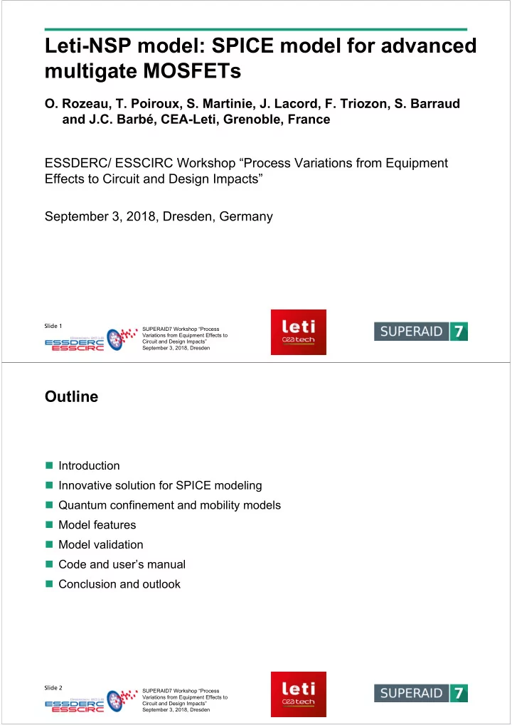
Leti-NSP model: SPICE model for advanced multigate MOSFETs O. Rozeau, T. Poiroux, S. Martinie, J. Lacord, F. Triozon, S. Barraud and J.C. Barbé, CEA-Leti, Grenoble, France ESSDERC/ ESSCIRC Workshop “Process Variations from Equipment Effects to Circuit and Design Impacts” September 3, 2018, Dresden, Germany Slide 1 SUPERAID7 Workshop “Process Variations from Equipment Effects to Circuit and Design Impacts” September 3, 2018, Dresden Outline Introduction Innovative solution for SPICE modeling Quantum confinement and mobility models Model features Model validation Code and user’s manual Conclusion and outlook Slide 2 SUPERAID7 Workshop “Process Variations from Equipment Effects to Circuit and Design Impacts” September 3, 2018, Dresden
Introduction Context: more Moore from International Roadmap for Devices and Systems LGAA = Vertically stacked NS/NW GAA MOSFET VGAA = Vertical NS/NW GAA MOSFET From irds.ieee.org: More Moore report 2017 edition Advanced Gate All Around (GAA) MOSFET are introduced for sub-7nm nodes: require SPICE models for IC design Slide 3 SUPERAID7 Workshop “Process Variations from Equipment Effects to Circuit and Design Impacts” September 3, 2018, Dresden Introduction Challenges of GAA MOSFET modeling IMEC, VLSI’16 IBM, VLSI’17 Leti, IEDM’16 1. GAA MOSFET can have different shapes: cylindrical, rectangular (sheet) 2. In the case of stack-GAA: the nanowires /nanosheets can have size differences Leti, IEDM’06 Slide 4 SUPERAID7 Workshop “Process Variations from Equipment Effects to Circuit and Design Impacts” September 3, 2018, Dresden
Introduction Our solution is Leti-NSP model dedicated to advanced multigate MOSFET. Leti-NSP model can simulate: Vertically stacked GAA MOSFET (nanosheet and/or nanowire) Vertical channel GAA MOSFET (nanosheet and/or nanowire) FinFET / Trigate MOSFET Vertically stacked Vertical channel FinFET/Trigate GAA MOSFET GAA MOSFET MOSFET Slide 5 SUPERAID7 Workshop “Process Variations from Equipment Effects to Circuit and Design Impacts” September 3, 2018, Dresden Introduction Model’s core: modeling of vertically stacked GAA is complex and challenging Main goals: find a compact formalism for Accuracy: physical approach CPU time efficiency: single instance Main difficulties: the surface potential is not constant along the NW/NS perimeter GAA can have different sizes: surface potentials are not the same for all GAA Illustration of vertically stacked GAA MOSFET: 3 Nanosheets Slide 6 SUPERAID7 Workshop “Process Variations from Equipment Effects to Circuit and Design Impacts” September 3, 2018, Dresden
Innovative Solution for SPICE Modeling Concept of Leti-NSP model: GAA MOSFET architecture and its asymptotic cases 2 asymptotic cases: Symmetrical double gate and cylindrical GAA MOSFET Slide 7 SUPERAID7 Workshop “Process Variations from Equipment Effects to Circuit and Design Impacts” September 3, 2018, Dresden Innovative Solution for SPICE Modeling Concept of Leti-NSP model: GAA MOSFET architecture and its asymptotic cases 1 - Unique model for these both asymptotic cases Common SPICE model 2 - Solution for stacked-nanosheet GAA MOSFET and vertical GAA MOSFET Slide 8 SUPERAID7 Workshop “Process Variations from Equipment Effects to Circuit and Design Impacts” September 3, 2018, Dresden
Innovative Solution for SPICE Modeling Asymptotic cases: unique equation (Poisson’s equation + boundary conditions) � � 4 ∙ ε �� See O. Rozeau et al, � � � � ∙ � � � � � � ∙ ��� � � � � IEDM’16 H ∙ C′ �� Cylindrical Planar SDG � �� � �� � � 2�� , � � � and �′ �� � � � 1μ� , � � � �� and �′ �� � �∙�� �� ��� � �� � Slide 9 SUPERAID7 Workshop “Process Variations from Equipment Effects to Circuit and Design Impacts” September 3, 2018, Dresden Innovative Solution for SPICE Modeling Nanosheet GAA MOSFET partitioning Outer parts: W ����� , C ���,����� Gate , H ����� Oxide Inner part: W ����� , C ���,����� W ��� � W ����� � W ����� Si T ch H � W ����� ∙ H ����� � W � T �� ∙ T �� W ��� W ��� C′ �� � W ����� ∙ C ���,����� � W � T �� ∙ C′ ��,����� T ch /2 T ch /2 W ��� W ��� W � � ε �� C �� H outer inner outer Innovative solution in NSP model: an unique effective surface potential is obtained by the resolution of an unified equation for nanosheet Slide 10 SUPERAID7 Workshop “Process Variations from Equipment Effects to Circuit and Design Impacts” September 3, 2018, Dresden
Innovative Solution for SPICE Modeling NSP-model can reproduced all GAA shapes without fitting parameters Slide 11 SUPERAID7 Workshop “Process Variations from Equipment Effects to Circuit and Design Impacts” September 3, 2018, Dresden Innovative Solution for SPICE Modeling Case of stacked-nanosheet GAA MOSFET � � � � ∙ � ���,� �′ �� � � � ����� ��� � � � � � � � ∙ � � � ����� ��� � � � ����� � � � � ��� The inversion charge is accurately and analytically modeled without fitting parameters Slide 12 SUPERAID7 Workshop “Process Variations from Equipment Effects to Circuit and Design Impacts” September 3, 2018, Dresden
Quantum Confinement and Mobility Models Case of stacked-nanosheet GAA MOSFET Blue: classical TCAD simulations Red: 2D Poisson-Schrödinger Simulations: TB_SIM • Effective mass: 6 bands k.p (higher than 10 sub-bands are solved) Quantum confinement has a significant impact on the inversion charge Slide 13 SUPERAID7 Workshop “Process Variations from Equipment Effects to Circuit and Design Impacts” September 3, 2018, Dresden Quantum Confinement and Mobility Models Dedicated compact model for GAA MOSFET (IEDM’16) Triangular-potential approximation (Stern 72) Structural confinement has a stronger impact on C inv in GAA than in planar bulk MOSFET For Leti-NSP model: dedicated solution including accurate modeling of Cgg slope without fitting parameter for the user Slide 14 SUPERAID7 Workshop “Process Variations from Equipment Effects to Circuit and Design Impacts” September 3, 2018, Dresden
Quantum Confinement and Mobility Models MODEL versus Simulations: Stacked-NS MOSFET (IEDM’16) Single effective mass: defined as a function of device polarity, Si orientation and Ge concentration for pFET without fitting parameters for users Slide 15 SUPERAID7 Workshop “Process Variations from Equipment Effects to Circuit and Design Impacts” September 3, 2018, Dresden Quantum Confinement and Mobility Models Mobility partitioning in GAA MOSFET In NSP model, 2 distinct mobility models is implemented for inner part and outer parts � � � ����� � �� �� � � � � � ∙ 1 � � ���� 1 � � �� ∙ � ��� � ��� � �� � ����� � �� ��� � �� � � �� ∙ 1 � � ���� 1 � � ��� ∙ � ��� � ��� Coulomb High field effect scattering For model accuracy, quantum confinement is included in the inversion charge and electrical field calculations Slide 16 SUPERAID7 Workshop “Process Variations from Equipment Effects to Circuit and Design Impacts” September 3, 2018, Dresden
Quantum Confinement and Mobility Models Model evaluation: nfet Electrical field dependence Width dependence Wide N-channel single NS Wide MOSFET At N inv =8x10 12 cm -2 Narrow Narrow W=8, 18, 98, 218nm Symbols: experimental data (Leti) Lines: Leti-NSP model Symbols: experimental data (Leti) N-channel single NS MOSFET Lines: Leti-NSP model Slide 17 SUPERAID7 Workshop “Process Variations from Equipment Effects to Circuit and Design Impacts” September 3, 2018, Dresden Quantum Confinement and Mobility Models Model evaluation: pfet Electrical field dependence Width dependence Narrow P-channel single NS MOSFET Wide Narrow Wide At N inv =8x10 12 cm -2 W=15, 20, 60, 220nm Symbols: experimental data (Leti) Lines: Leti-NSP model Symbols: experimental data (Leti) Lines: Leti-NSP model P-channel single NS MOSFET Slide 18 SUPERAID7 Workshop “Process Variations from Equipment Effects to Circuit and Design Impacts” September 3, 2018, Dresden
Overview of Model Features For all device sizes Model features: Leti-NSP model v1.0.0 Interface states Quantum mechanical effect (confinement) Mobility model Channel doping effect including sidewall Management of SiGe channel for pfet effects Mobility model including sidewall effects Temperature scaling and self-heating effect Channel doping effect Quantum confinement modeling Slide 19 SUPERAID7 Workshop “Process Variations from Equipment Effects to Circuit and Design Impacts” September 3, 2018, Dresden Overview of Model Features Short channel effects Model features: Leti-NSP model v1.0.0 Threshold voltage roll-off L-scaling of mobility model Drain Induced Barrier Lowering Velocity saturation Channel length modulation in saturation Series resistances with bias dependence Slide 20 SUPERAID7 Workshop “Process Variations from Equipment Effects to Circuit and Design Impacts” September 3, 2018, Dresden
Recommend
More recommend
Explore More Topics
Stay informed with curated content and fresh updates.
