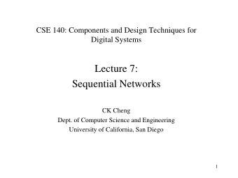
Lecture 7: Sequential Networks CSE 140: Components and Design - PowerPoint PPT Presentation
Lecture 7: Sequential Networks CSE 140: Components and Design Techniques for Digital Systems Spring 2014 CK Cheng, Diba Mirza Dept. of Computer Science and Engineering University of California, San Diego 1 Sequential Networks Memory
Lecture 7: Sequential Networks CSE 140: Components and Design Techniques for Digital Systems Spring 2014 CK Cheng, Diba Mirza Dept. of Computer Science and Engineering University of California, San Diego 1
Sequential Networks • Memory Components – Hierarchy of Memory – Basic Mechanism of Memory – Types of Flip-Flops • Implementation – Finite State Machine 2
Part II. Sequential Networks (Ch. 3) Memory / Time steps s i x i y i y i =f i (S t ,X) Clock s i t+1 =g i (S t ,X) Memory: Flip flops Specification: Finite State Machines Implementation: Excitation Tables 3
What is a sequential circuit? “A circuit whose output depends on current inputs and past outputs” “A circuit with memory” 4
Why do we need circuits with ‘memory’? A. Complex systems often consist of circuits that perform a sequence of tasks B. Circuits with memory can be used to store data C. Both A and B 5
The connection between sequences and memory • What differentiates a musical piece from a cacophony? • What is the role of memory in playing a musical piece (essentially a sequence of notes)? 6
Sequential Network vs. Combinational Logic: Q: Which of the following is FALSE? A. Combinational logic can replace any sequential network to realize the same function. B. Sequential networks use the same set of logic gates as combinational logic. C. Sequential networks can implement a CPU. D. Sequential networks require a precise clock for timing. 7
Hierarchy of Memory Devices • Memory Bank (Farms of memory cells) • Register (Vector of memory cells) • Flip-Flop (Single memory cell) – SR, D, T, JK flip-flops (Different types of memory cells) – State Tables (Truth table of sequential machine) – Characteristic Expressions (Switching algebraic expression of sequential machine) 8
Fundamental Memory Mechanism I1 Q Q Q I2 I1 I2 Q 9
Memory Mechanism: Capacitive Load • Fundamental building block of sequential circuits • Two outputs: Q , Q • There is a feedback loop! • In a typical combinational logic, there is no feedback loop. • No inputs I1 Q Q Q I2 I1 I2 Q 10
Capacitive Loads • Consider the two possible cases: – Q = 0: then Q’ = 1 and Q = 0 (consistent) 0 I1 Q 1 0 1 I2 Q – Q = 1: then Q ’ = 0 and Q = 1 (consistent) 1 I1 Q 0 1 0 I2 Q – Bistable circuit stores 1 bit of state in the state variable, Q (or Q’ ) • But there are no inputs to control the state 11
iClicker Q. Given a memory component made out of a loop of inverters, the number of inverters has to be A. Even B. Odd 12
SR (Set/Reset) Latch • SR Latch R N1 Q N2 Q S • Consider the four possible cases: – S = 1, R = 0 – S = 0, R = 1 – S = 0, R = 0 – S = 1, R = 1 13
SR Latch Analysis – S = 1, R = 0: 0 R N1 Q 1 N2 Q S 1 – S = 0, R = 1: R N1 Q 0 N2 Q S 14
SR Latch Analysis – S = 1, R = 0: then Q = 1 and Q = 0 0 R N1 Q 1 N2 Q S – S = 0, R = 1: then Q = 0 and Q = 1 1 R N1 Q 0 N2 Q S 15
SR Latch Analysis – S = 1, R = 1: 1 R N1 Q 1 N2 Q S 16
SR Latch Analysis – S = 0, R = 0: R N1 Q N2 Q S 17
SR Latch Analysis – S = 0, R = 0: then Q = Q prev Q prev = 0 Q prev = 1 0 0 R 0 R N1 Q N1 Q 0 N2 Q 0 N2 Q S S – S = 1, R = 1: then Q = 0 and Q = 0 1 R N1 Q 1 N2 Q S 18
y S y = (S+Q)’ Q Q = (R+y)’ R 19
Flip-flop Components SR F-F (Set-Reset) y S R Q Inputs: S, R State: (Q, y) 20
Id Q(t) y(t) S R Q(t 1 ) y(t 1 ) Q(t 2 )y(t 2 ) Q(t 3 ) y(t 3 ) State 0 0 0 0 0 1 1 0 0 1 1 1 0 0 0 1 0 1 0 1 0 1 Q y 2 0 0 1 0 1 0 1 0 1 0 3 0 0 1 1 0 0 0 0 0 0 SR 4 0 1 0 0 0 1 0 1 0 1 Transition 5 0 1 0 1 0 1 0 1 0 1 6 0 1 1 0 0 0 1 0 1 0 7 0 1 1 1 0 0 0 0 0 0 State Diagram 8 1 0 0 0 1 0 1 0 1 0 00 9 1 0 0 1 0 0 0 1 0 1 01 10 00 10 1 0 1 0 1 0 1 0 1 0 10 01 10 10 01 11 1 0 1 1 0 0 0 0 0 0 11 12 1 1 0 0 0 0 1 1 0 0 10 01 11 13 1 1 0 1 0 0 0 1 0 1 10 00 SR 14 1 1 1 0 0 0 1 0 1 0 11 01 15 1 1 1 1 0 0 0 0 0 0 00 00 11 11 21
CASES: SR=01, (Q,y) = (0,1) SR=10, (Q,y) = (1,0) SR=11, (Q,y) = (0,0) SR = 00 => if (Q,y) = (0,0) or (1,1), the output keeps changing Q. To avoid the SR latch output from toggling or behaving in an undefined way which input combinations should be avoided: A. (S, R) = (0, 0) B. (S, R) = (1, 1) 22
SR Latch Analysis – S = 0, R = 0: then Q = Q prev and Q = Q prev (memory!) Q prev = 0 Q prev = 1 0 0 R 0 R 1 N1 Q N1 Q 1 0 0 1 1 0 0 N2 Q 0 N2 Q S S – S = 1, R = 1: then Q = 0 and Q = 0 (invalid state: Q ≠ NOT Q ) 1 R 0 N1 Q 0 0 0 1 N2 Q S 23
CASES: SR=01, (Q,y) = (0,1) SR=10, (Q,y) = (1,0) SR=11, (Q,y) = (0,0) SR = 00 => if (Q,y) = (0,0) or (1,1), the output keeps changing Solutions: 1) SR = (0,0), or 2) SR = (1,1). State table SR inputs 00 01 10 11 PS 0 0 0 1 - Characteristic Expression Q(t) 1 1 0 1 - Q(t+1) = S(t)+R’(t)Q(t) Q(t+1) NS (next state) 24
SR Latch Symbol • SR stands for Set/Reset Latch – Stores one bit of state ( Q ) • Control what value is being stored with S , R inputs – Set: Make the output 1 ( S = 1, R = 0, Q = 1 ) – Reset: Make the output 0 ( S = 0, R = 1, Q = 0 ) SR Latch • Must do something to avoid Symbol invalid state (when S = R = 1) R Q S Q 25
D Latch • Two inputs: CLK , D – CLK : controls when the output changes – D (the data input): controls what the D Latch output changes to Symbol • Function CLK – When CLK = 1, D passes through to Q D Q (the latch is transparent ) – When CLK = 0, Q holds its previous Q value (the latch is opaque ) • Avoids invalid case when Q ≠ NOT Q 26
D Latch Internal Circuit SR Latch Symbol CLK R Q D Q S Q Q 27
D Latch Internal Circuit CLK CLK R R Q Q D D Q S S Q Q D Q CLK D D S R Q Q 0 X 1 0 1 1 28
D Latch Internal Circuit CLK CLK R R Q Q D D Q S S Q Q Q D CLK D D S R Q Q 0 X X 0 0 Q prev Q prev 1 0 1 0 1 0 1 1 1 0 1 0 1 0 29
D Flip-Flop • Two inputs: CLK , D • Function – The flip-flop “samples” D on the rising D Flip-Flop edge of CLK Symbols • When CLK rises from 0 to 1, D passes through to Q • Otherwise, Q holds its previous value D Q – Q changes only on the rising edge of CLK Q • A flip-flop is called an edge-triggered device because it is activated on the clock edge 30
D Flip-Flop Internal Circuit CLK CLK CLK N1 D D Q D Q Q L1 Q L2 Q Q 31
D Flip-Flop Internal Circuit • Two back-to-back latches (L1 and L2) controlled by complementary clocks • When CLK = 0 CLK CLK – L1 is transparent, L2 is opaque – D passes through to N1 CLK CLK CLK CLK N1 N1 • When CLK = 1 D D D D Q Q D D Q Q Q Q L1 L1 Q Q L2 L2 Q Q Q Q – L2 is transparent, L1 is opaque – N1 passes through to Q • Thus, on the edge of the clock (when CLK rises from 0 1) – D passes through to Q 32
D Flip-Flop vs. D Latch CLK D Q D Q Q Q CLK D Q (latch) Q (flop) 33
D Flip-Flop vs. D Latch CLK D Q D Q Q Q CLK D Q (latch) Q (flop) 34
Latch and Flip-flop (two latches) A latch can be considered as a door CLK = 0, door is shut CLK = 1, door is unlocked A flip-flop is a two door entrance CLK = 1 CLK = 0 CLK = 1 35
D Flip-Flop (Delay) CLK Q D CLK CLK N1 CLK D D Q D Q Q Q’ L1 Q L2 Q Q Id D Q(t) Q(t+1) State table 0 0 0 0 PS D 0 1 1 0 1 0 0 0 1 2 1 0 1 1 0 1 3 1 1 1 NS= Q(t+1) Characteristic Expression: Q(t+1) = D(t) 36
iClicker Can D flip-flip serve as a memory component? A. Yes B. No 37
JK F-F State table Q J JK 00 01 10 11 PS CLK 0 0 0 1 ? Q’ K 1 1 0 1 ? Q(t+1) 38
JK F-F State table Q J JK 00 01 10 11 PS CLK 0 0 0 1 1 Q’ K 1 1 0 1 0 Q(t+1) Characteristic Expression Q(t+1) = Q(t)K’(t)+Q’(t)J(t) 39
T Flip-Flop (Toggle) State table Q T PS T 0 1 CLK 0 0 1 Q’ 1 1 0 Q(t+1) Characteristic Expression Q(t+1) = Q’(t)T(t) + Q(t)T’(t) 40
Using a JK F-F to implement a D and T F-F Q x J CLK Q’ K iClicker What is the function of the above circuit? A. D F-F B. T F-F C. None of the above 41
Using a JK F-F to implement a D and T F-F Q T J CLK Q’ K T flip flop 42
Reading [Harris] Chapter 3: 3.3, 3.4.1, 3.4.2 43
Recommend
More recommend
Explore More Topics
Stay informed with curated content and fresh updates.

