Sequential Circuits Combinational circuits : current input output - PDF document
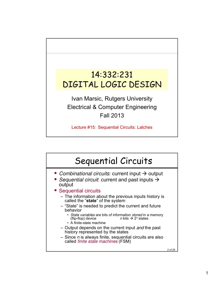
14:332:231 DIGITAL LOGIC DESIGN Ivan Marsic, Rutgers University Electrical & Computer Engineering Fall 2013 Lecture #15: Sequential Circuits: Latches Sequential Circuits Combinational circuits : current input output Sequential
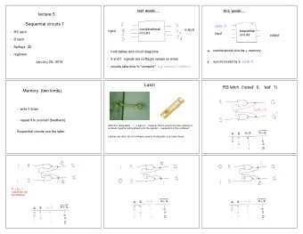
14:332:231 DIGITAL LOGIC DESIGN Ivan Marsic, Rutgers University Electrical & Computer Engineering Fall 2013 Lecture #15: Sequential Circuits: Latches Sequential Circuits Combinational circuits : current input output Sequential circuit : current and past inputs output Sequential circuits – The information about the previous inputs history is called the “ state ” of the system – “State” is needed to predict the current and future behavior • State variables are bits of information stored in a memory n bits 2 n states (flip-flop) device • A finite-state machine – Output depends on the current input and the past history represented by the states – Since n is always finite, sequential circuits are also called finite state machines (FSM) 2 of 29 1
Describing Sequential Circuits inputs output Combinational circuit State memory State table – For each current-state, specify next-states as function of inputs and current state State diagram – Graphical version of state table 3 of 29 Bistable Element The simplest sequential circuit Signal B = A appears after a short delay t pd = propagation delay B = A C = A A feedback: reinforces the input A A t pd B t pd C 4 of 29 2
Bistable Element The simplest sequential circuit No input… for the moment Two states = one Boolean state variable, say, “Q” B = A C = A A “twisted” V in2 V out2 representation: V in1 V out1 Q (Q_L is active low) V in2 V out2 Q_L 5 of 29 Bistable Element Assume Q is equal “0” LOW LOW V in1 V out1 Q Q V in2 V out2 Q_L Q_L LOW Bottom inverter’s HIGH output top inverter’s input LOW HIGH LOW Q Q Q_L Q_L LOW HIGH LOW HIGH Top inverter’s output is forced LOW 6 of 29 3
Bistable Element Assume Q is equal “0” LOW HIGH V in1 V out1 Q V in2 V out2 Q_L LOW HIGH Now assume Q is equal “1” LOW HIGH V in1 V out1 Q V in2 V out2 Q_L HIGH LOW 7 of 29 Analog Analysis (1) Assume pure CMOS thresholds, 5V is the V CC Theoretical threshold center is 2.5V In principle, any TTL/CMOS have the same behavior, but different constants … V OUT 5.0 HIGH 3.5 V in2 V out2 undefined 1.5 LOW 0 V IN 0 1.5 3.5 5.0 undefined LOW HIGH [ Recall Lecture #9 ] 8 of 29 4
Analog Analysis (2) Assume threshold inputs at 2.5 V: 2.5 V 2.5 V V in1 V out1 Q If nothing moves … but a little input noise moves Q for example to … V in2 V out2 Q_L 2.5 V 2.5 V LOW HIGH V in1 V out1 Q … Q is equal “1” V in2 V out2 Q_L HIGH LOW 9 of 29 Metastability Metastability is inherent in any bistable circuit Transfer function: stable V out1 V in1 = V out2 = V in2 = T ( V in2 ) metastable V in1 V out1 Q = T ( V out1 ) = T ( T ( V in1 )) V in2 V out2 Q_L stable V in2 = T ( T ( V in2 )) V in1 = V out2 Two stable points, one metastable point 10 of 29 5
Another Look at Metastability metastable stable stable If the ball sits exactly on the top of the hill, the bistable circuit can be in metastable state until random noise nondeterministically chooses one of the stable states. Can appear in any sequential circuit, as we will see … 11 of 29 Latches and Flip-Flops The two most popular varieties of elements used to build sequential circuits are: latches and flip- flops Latch: level sensitive storage element Flip-Flop: edge triggered storage element Common examples of latches: S-R latch, S-R latch, D latch (= gated D latch) Common examples of flip-flops (FF): D-FF, D-FF with enable, Scan-FF, JK-FF, T-FF 12 of 29 6
S-R Latch V in1 V out1 X Y X NOR Y Q 0 0 1 0 1 0 V in2 V out2 Q_L 1 0 0 1 1 0 S-R (Set-Reset) latch with NOR – similar to inverter pair, with capability to force output to “0” (Reset=1) or “1” (Set=1) Inputs Outputs R Q S R Q QN 0 0 last Q last QN (hold) (reset) 0 1 0 1 QN S 1 0 1 0 (set) (forbidden) 1 1 0 0 S Q S Q S Q R QN R Q R QN 13 of 29 S-R Latch Operation X Y X NOR Y 0 0 1 0 1 0 R Q 1 0 0 1 1 0 QN S S 0 1 0 0 ? Hold: 0 S QN = 1 0 R 0 0 0 1 ? R S 0 Q = 0 before Q R after = 0 QN Q 0 1 1 0 ? ε ε 0 Set: QN = 0 t t 1 t 2 t 3 t 4 1 S 0 Q = 0 t 1 + ε t 3 + ε R = 1 Hold: 1 S(t) R(t) Q(t) Q(t+ ε ) QN(t+ ε ) QN = 0 0 0 0 0 0 1 S 0 0 0 1 1 0 Q = 1 R = 1 0 1 0 0 1 0 1 1 0 1 1 0 0 1 0 Reset: 1 QN = 0 1 0 1 1 0 0 S 1 1 0 Still to analyze 1 Still to analyze Q = 1 R 1 1 1 = 0 14 of 29 7
S-R Latch Operation Typical operation of an S-R Latch (a) “normal” inputs set reset (a) S Inputs Outputs S R Q QN R 0 0 last Q last QN (hold) Q (reset) 0 1 0 1 (set) 1 0 1 0 QN (forbidden) 1 1 0 0 hold 15 of 29 S-R Latch Operation Typical operation of an S-R Latch (a) “normal” inputs (b) S and R asserted simultaneously (a) S Inputs Outputs S R Q QN R 0 0 last Q last QN (hold) Q (reset) 0 1 0 1 (set) 1 0 1 0 QN (forbidden) 1 1 0 0 S R (b) Q QN Both Q and QN are “0” simultaneously 16 of 29 8
S-R Latch Operation Typical operation of an S-R Latch (a) “normal” inputs (b) S and R asserted simultaneously (a) S R Q Metastability is possible if S and R are negated QN simultaneously S “race R (b) condition” Q QN say, less than 20ns 17 of 29 Improper S-R Latch Operation Metastability may occur if S and R are negated simultaneously: the circuit starts to oscillate 1 0 R 0 1 0 1 Q QN 0 1 0 1 S 1 0 not allowed !!! set reset S “race R (b) condition” Q QN hold 18 of 29 9
S-R Latch Timing Parameters Propagation delay ( t p ) for an input transition to produce an output Minimum pulse width ( t pw ) needed for deterministic transitions S (1) R (2) Q S or R impulse is t pLH(SQ) t pHL(RQ) t pw(min) less than t pw also leads to metastability Recovery time ( t rec ) = minimum delay between negating S and R for them not to be considered simultaneous t rec and t pw are related: both measure how long it takes for the latch feedback loop to stabilize Violations of t pw and t rec cause metastability 19 of 29 R-S Latch Analysis ■ Break the feedback path R Q(t) QN Q S(t) Q(t+ ∆ ) R(t) QN S Q(t+ ∆ ): Inputs Output S(t) R(t) Q(t) Q(t+ ∆ ) S(t) S(t) S(t)R(t) 0 0 0 0 (hold) Q(t) 0 0 1 1 00 01 11 10 0 1 0 0 0 2 6 4 (reset) 0 0 0 x 1 0 1 1 0 1 0 0 1 1 3 7 5 1 1 0 x 1 Q(t) (set) 1 0 1 1 1 1 0 x (not allowed) R(t) R (t)·Q(t) 1 1 1 x ■ Next state equation, a.k.a. characteristic equation : Q + = Q = S + R ·Q Q(t+ ∆ ) = S(t) + R (t)·Q(t) 20 of 29 10
Theoretical R-S Latch Behavior R Q State diagram QN S – states : S R = 0 0 possible values S R = 1 0 S R = 0 1 S R = 0 0 – transitions : S R = 1 0 changes based Q QN S R = 0 1 Q QN on inputs 1 0 0 1 S R = 1 0 S R = 0 1 S R = 1 1 1 1 = R S R = 1 1 S Q QN 0 0 S R = 0 0 S R = 0 1 S R = 1 0 S R = 1 1 S R = 0 0 possible oscillation Q QN between states “0 0” and “1 1” 1 1 21 of 29 Observed R-S Latch Behavior R Q Very difficult to QN S observe R-S latch in the 1-1 state S R = 0 0 – one of R or S S R = 1 0 S R = 0 1 S R = 0 0 usually changes S R = 1 0 first Q QN Ambiguously returns S R = 0 1 Q QN 1 0 to state 0-1 or 1-0 0 1 S R = 1 0 – a so-called "race S R = 0 1 metastability condition" S R = 1 1 1 – or non- 1 = deterministic R S R = 1 1 transition Q QN S 0 0 S R = 0 0 S R = 0 0 22 of 29 11
S-R Latch using NAND gates Used more than S-R latch with NOR … because NAND gates are preferred over NOR gates S_L or S Q S Q R Q R_L QN or S Inputs Outputs S_L R_L Q QN Timing and metastability 0 0 1 1 similar as for S-R 0 1 1 0 1 0 0 1 1 1 last Q last QN ■ Next state equation (characteristic equation): Q(t+ ∆ ) = S (t) + R(t)·Q(t) Q + = Q = S + R·Q 23 of 29 Bistable Application: Switch Debouncing Mitigating oscillations in mechanical switches when the wiper makes contact with the terminal push Problem if the switch is used for counting the number of pushes Wakerly, Section 8.2.3 24 of 29 12
Recommend
More recommend
Explore More Topics
Stay informed with curated content and fresh updates.
