Modeling Synchronous Logic Circuits Debdeep Mukhopadhyay IIT - PowerPoint PPT Presentation
Modeling Synchronous Logic Circuits Debdeep Mukhopadhyay IIT Madras Basic Sequential Circuits A combinational circuit produces output solely depending on the current input. But a sequential circuit remembers its previous state.
Modeling Synchronous Logic Circuits Debdeep Mukhopadhyay IIT Madras
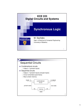
Basic Sequential Circuits • A combinational circuit produces output solely depending on the current input. • But a sequential circuit “remembers” its previous state. • Its output depends on present inputs and previous state. • Examples: – Latches – Registers – Memory – parallel to serial / serial to parallel converters – Counters
Latch vs Registers • Latch: Level sensitive device – Positive Latches and Negative latches – Can be realized using multiplexers • Register: edge triggered storage element – Can be implemented using latches – Cascade a negative latch with a positive latch to obtain a positive edge triggered register • Flip flop: bi-stable component formed by the cross coupling of gates.
Latches • Cycle stealing is possible leading to faster circuits • Problem of timing analysis.
Latch inference using if A1 D Q • module …. Y1 G ~Q always@(...) En1 begin C2 if(En1) D Q A2 Y1=A1; G ~Q Y2 D Q if(En2) B2 G ~Q begin M2<=!(A2&B2); En2 Y2<=!(M2|C2); end C3 if(En3) Y3 A3 begin D Q M3=!(A3&B3); B3 G ~Q Y3=!(M3|C3); end En3
Modeling latches with present and clear inputs • begin • begin if(!Clear1) if(Clear2) Y1=0; Y2=0; else if(En) else if(En) Y1=A1; Y2=A2;
Modeling latches with present and clear inputs • if(!Preset3) • if(!Preset3) Y3=1; Y3=1; else if(En3) else if(En3) Y3=A3; Y3=A3; D Q G ~Q CLR
Modeling latches with present and clear inputs A5 • if(Clear5) Y5 D Q En5 Y5=0; G ~Q else if(Preset5) CLR Y5=1; Preset5 else if(En5) Y5=A5; Clear5 If there are no latches with a preset input In the library, equivalent functionality is produced by using latches with a clear input.
Multiple gated latch always @(En1 or En2 or En3 …) if(En1==1) Try to synthesize and check whether: Y=A1; 1. Is there a latch inferred? else if(En2==1) 2. Put an else statement. Is a latch inferred now? Y=A2; 3. Put a default output assignment else if(En3==1) before the if starts. Is a latch inferred now? Y=A3; 4. Use the posedge keyword in the trigger list, and repeat the above experiments.
Other places of latch inferences • Nested if: If all the possibilities are not mentioned in the code. • Case: In advertent. Not advisable to infer a latch from case statement. – may lead to superfluous latches. • Nested case statements can also infer latches.
The D-Flip Flop • always @(posedge clk) Y=D; • A-Synchronous reset: always @(posedge clk or posedge reset) if(reset) Y=0 else Y=D;
Resets • Synchronous reset: always @(posedge clk) if(reset) Y=0 else Y=D;
Combinational Block between two flops • always@(posedge clk) begin M <= !(A & B); Y <= M|N; end assign N=C|D; What will happen if a blocking assignment is used? The first flip flop will become redundant…
Sequence Generators • Linear Feedback Shift Registers • Counters
LFSR Applications • Pattern Generators • Counters • Built-in Self-Test (BIST) • Encryption • Compression • Checksums • Pseudo-Random Bit Sequences (PRBS)
LFSR � Linear Feedback Shift Register (LFSR): � For pseudo random number generation � A shift register with feedback and exclusive-or gates in its feedback or shift path. � The initial content of the register is referred to as seed . � The position of XOR gates is determined by the polynomial ( poly ).
An LFSR outline The feedback function (often called the taps) can be reprsesented by a polynomial of degree n
A 4 bit LFSR The feedback polynomial is p(x)=x 4 +x+1
A 4 bit LFSR 1111 0111 1011 0101 1010 1101 0110 0011 1001 0100 0010 0010 1000 Output sequence: 1100 111101011001000... 1110 All the 2 4 -1 possible states are generated. This is called a maximal length LFSR. So, the sequence depends on the feedbacks.
Types of feedbacks • Feedbacks can be comprising of XOR gates. • Feedbacks can be comprising of XNOR gates. • Given the same tap positions, both will generate the same number of values in a cycle. But the values will be same. • Permutation!
Number of Taps • For many registers of length n, only two taps are needed, and can be implemented with a single XOR (XNOR) gate. • For some register lengths, for example 8, 16, and 32, four taps are needed. For some hardware architectures, this can be in the critical timing path. • A table of taps for different register lengths is included in the back of this module.
One-to-Many and Many-to- One Implementation (a) has only a single gate delay between flip-flops.
Avoiding the Lockup State Will Use XOR Form For Examples We have an n-bit LFSR, shifting to the “right” n 0
Avoiding the Lockup State Will Use XOR Form For Examples The all ‘0’s state can’t be entered during normal operation but we can get close. Here’s one of n examples: 0 0 0 0 0 1 n 0 We know this is a legal state since the only illegal state is all 0’s. If the first n-1 bits are ‘0’, then bit 0 must be a ‘1’.
Avoiding the Lockup State Will Use XOR Form For Examples Now, since the XOR inputs are a function of taps, including the bit 0 tap, we know what the output of the XOR tree will be: ‘1’. It must be a ‘1’ since ‘1’ XOR ‘0’ XOR ‘0’ XOR ‘0’ = ‘1’. 0 0 0 0 0 1 n 0 So normally the next state will be: 1 0 0 0 0 0 n 0
Avoiding the Lockup State Will Use XOR Form For Examples But instead, let’s do this, go from this state: 0 0 0 0 0 1 n 0 To the all ‘0’s state: 1 0 0 0 0 0 n 0
Avoiding the Lockup State Modification to Circuit 2 n-1 states 2 n states NOR of all bits except bit 0 Added this term a) “000001” : 0 Xor 0 Xor 0 Xor 1 Xor 1 ⇒ 0 0 Xor 0 Xor 0 Xor 0 Xor 1 ⇒ 1 b) “000000” : c) “100000” :
Verilog code module … always@(posedge clk or posedge rst) begin if(rst) LFSR_reg=8’b0; else LFSR_reg=Next_LFSR_reg; end
verilog always @(LFSR_reg) begin Bits0_6_zero=~|LFSR_Reg[6:0]; Feedback=LFSR_Reg[7]^ Bits0_6_zero; for(N=7;N>0;N=N-1) if(Taps[N-1]==1) Next_LFSR_Reg[N]=LFSR_Reg[N-1]^Feedback; else Next_LFSR_Reg[N]=LFSR_Reg[N-1]; Next_LFSR_Reg[0]=Feedback; end assign Y=LFSR_Reg; endmodule
A Generic LFSR module LFSR_Generic_MOD(Clk,rst,Y); parameter wdth=8; input clk,rst; output [wdth-1:0] Y; reg [31:0] Tapsarray [2:32]; wire [wdth-1:0] Taps; integer N; reg Bits0_Nminus1_zero, Feedback; reg [wdth-1:0] LFSR_Reg, Next_LFSR_Reg;
always @(rst) begin TapsArray[2]=2’b11; TapsArray[3]=3’b101; … TapsArray[32]=32’b10000000_00000000_00000000_01100010; end assign Taps[wdth-1:0]=TapsArray[wdth]; REST OF THE CODE IS SIMILAR TO THE PREVIOUS EXAMPLE
Counters • A register that goes through a pre- determined sequence of binary values (states), upon the application of input pulses in one or more than inputs is called a counter. • The input pulses can be random or periodic. • Counters are often used as clock dividers.
Timing Diagrams • The outputs (Q0 ⇒ Q3) of the counter can be used as frequency dividers with Q0 = Clock ÷ 2, Q1 = Clock ÷ 4, Q2 = Clock ÷ 8, and Q3 = Clock ÷ 16.
Types • Synchronous – Using adders, subtractors – Using LFSRs, better performance because of simple circuits. Most feedback polynomials are trinomials or pentanomials. • Asynchronous: – Ripple through flip flops – each single flip flop stage divides by 2 – so, we may obtain division by 2 n – what if they are not powers of two? we require extra feedback logic – significantly smaller
Divide by 13 : A synchronous design always@(posedge clk or posedge rst) begin if(!rst) begin cnt<=startcnt; Y<=0; end
Divide by 13 : A synchronous design else if(Count==EndCount) begin Count<=StartCount; Y<=1; end
Divide by 13 : A synchronous design else begin for(N=1;N<=3;N=N-1) if(Taps[N]) Count[N]<=Count[N-1]~^Count[3]; else Count[N]<=Count[N-1]; Count[0]<=Count[3]; Y=0; end end
Asynchronous Design • Instantiate 4 DFFs. • Ripple the clock through them • Output is a divided by 16 clock. • Use the output states and check when 13 clock cycles have elapsed. • Use it to make the output bit high. • Reset the Flip Flops • Exercise: Write a verilog code!
Pros and Cons of Synchronous and Asynchronous Resets
Problem of Choice • Quite a complex issue. • All of us know the importance of the reset button. When our PC does not work! • Less understood, less emphasized. • Require to a treatment to perform an informed design.
Some Points • Reset style depends on the ASIC design style, the application and where the flip flop is located. • If we design considering all the unused states (like the 2 n -2n states in a Johnson’s Counter), we should be able to do reset from any possible state. • A power on reset is required if the designer used the unused states as don’t cares to do optimization. • Often an explicit reset is not required if the flop is a part of shift register, just wait for some clock cycles. These are often called follower flops
Recommend
More recommend
Explore More Topics
Stay informed with curated content and fresh updates.
