Lecture 4: Sequential Circuits Continued Clock signals Clocks are - PowerPoint PPT Presentation
Lecture 4: Sequential Circuits Continued Clock signals Clocks are a regular pulse signal, where the high value indicates that the output of the latch may be sampled. Usually drawn as: voltage 5V time But looks more like:
Lecture 4: Sequential Circuits Continued
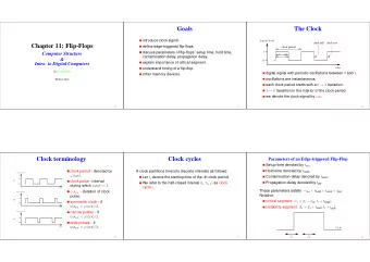
Clock signals § “Clocks” are a regular pulse signal, where the high value indicates that the output of the latch may be sampled. § Usually drawn as: voltage 5V time § But looks more like:
Signal restrictions § What’s the limit to how fast the latch circuit can be sampled? § Determined by: ú latency time of transistors Setup and hold time ú setup time for clock signal Jitter Gibbs phenomenon § Frequency = how many pulses occur per second, measured in Hertz (or Hz).
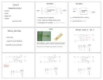
Clocked SR latch S Q C Q R § Adding another layer of NAND gates to the SR latch gives us a clocked SR latch or gated SR latch) ú Basically, a latch with a control input signal C . § The input C is often connected to a pulse signal that alternates regularly between 0 and 1 ( clock )
Clocked SR latch behaviour 0 1 § Same behaviour as SR 0 S latch, but with timing: Q 1 C ú Start off with S = 0 and R = 1 , like earlier example. Q R 1 ú If clock is high, the first 0 1 NAND gates invert those 0 values, which get inverted 1 0 S again in the output. Q 1 ú Setting both inputs to 0 C maintains the output Q values. R 1 0 1 0 1
Clocked SR latch behaviour 0 1 1 § Continued from previous: 0 S Q 0 1 ú Now set the clock low. C ú Even if the inputs change, Q the low clock input R 1 prevents the change from 1 1 0 reaching the second stage 0 1 of NAND gates. 1 1 0 S ú Result: the clock needs to Q 0 be high in order for the C inputs to have any effect. Q R 1 1 1 0
Clocked SR latch S Q S Q C C R Q Q R § This is the typical symbol for a clocked SR latch. § This only allows the S and R signals to affect the circuit when the clock input ( C ) is high. § Note: the small NOT circle after the Q output is simply the notation to use to denote the inverted output value. It’s not an extra NOT gate.
Clocked SR latch behaviour S Q T S R Q T+1 Result Q 0 0 0 0 no change C 0 0 1 0 reset 0 1 0 1 set Q 0 1 1 ? ??? R 1 0 0 1 no change 1 0 1 0 reset § Wait! 1 1 0 1 set 1 1 1 ? ??? § Where’s the clock? § There’s a better way to look at this….
Clocked SR latch behaviour C S R Q T+1 Result S Q 0 X X Q T no change 1 0 0 Q T no change C 1 0 1 0 reset Q 1 1 0 1 set R 1 1 1 ? Undefined § Assuming the clock is 1 , we still have a problem when S and R are both 1 , since the state of Q is indeterminate. ú Better design: prevent S and R from both going high.
D latch Q T D Q T+1 D Q 0 0 0 0 1 1 C 1 0 0 Q 1 1 1 § By making the inputs to R and S dependent on a single signal D , you avoid the indeterminate state problem. § The value of D now sets output Q low or high whenever C is high.
D latch D Q D Q C C Q Q § This design is good, but still has problems. ú i.e. timing issues. ú How can we maintain state?
Latch timing issues § Consider the circuit on the right: D Q C § When the clock signal Q is high, the output looks like the waveform below: ú Output keeps toggling back and forth. C …what happens next? Q
Latch timing issues § Consider the circuit on the right: D Q C § When the clock signal Q is high, the output looks like the waveform below: ú Output keeps toggling back and forth. C Q
D-Latch is transparent! § Transparent means that ú Any changes to its inputs are visible to the output when control signal (Clock) is 1. § Key Take-away: The “output of a latch should not be applied directly or through combinational logic to the input of the same or another latch when they all have the same control (clock) signal.”
Latch timing issues § Preferable behaviour: ú Have output change only once when the clock pulse changes. ú Solution: create disconnect between circuit output and circuit input, to prevent unwanted feedback and changes to output. S Q S Q C C R Q R Q
SR master-slave flip-flop § A flip-flop is a latched circuit whose output is triggered with the rising edge or falling edge of a clock pulse. § Example: The SR master-slave flip-flop S Q S 0 Q S 1 Q C C C R Q R 0 Q R 1 Q
SR master-slave flip-flop S Q S 0 Q 0 S 1 Q 1 C C C R Q R 0 Q 0 R 1 Q 1 C S propa- R gation delay Q
Edge-triggered D flip-flop § SR flip-flops still have issues of unstable behaviour. § Solution: D flip-flop ú Connect D latch to the input of a SR latch. ú Negative-edge triggered flip-flop (like the SR) D Q D Q S Q C C C Q Q R Q
Flip-flop behaviour 0 Z 0 § Observe the behaviour: D Q Q Q D S C ú If the clock signal is high, the C C Q 1 Q Q R input to the first flip-flop is Z sent out to the second. 0 ú The second flip-flop doesn’t do anything until the clock 0 0 0 signal goes down again. D Q D Q S Q ú When it clock goes from high C C C to low, the first flip-flop Q 0 1 Q Q R stops transmitting a signal, 1 1 0 and the second one starts.
Flip-flop behaviour 0 0 0 1 § Continued from previous: D Q Q Q D S C C C ú If the input to D changes, Q 0 Q Q R the change isn’t 1 transmitted to the second 1 flip-flop until the clock goes high again. 0 1 0 0 1 ú Once the clock goes high, D Q D Q S Q C C C the first flip-flop starts Q 0 1 Q Q R transmitting at the same 1 1 time as the second flip- 0 1 flop stops.
Confused yet? § Maybe a demonstration will help
Edge-triggered flip-flop § Alternative: positive-edge triggered flip-flops D Q D Q S Q D Q C C C C Q Q R Q Q § These are the most commonly-used flip-flop circuits (and our choice for the course).
Notation S S D D § Latches R R C C SR D with 0 D with 1 SR Control Control § Master-slave S S D D D D C C flip-flops C R R C C C Triggered SR Triggered D Triggered D Triggered SR § Edge-triggered D D Note: While all these are possible, we flip-flops mainly use edge- C C triggered D flip-flops Triggered D Triggered D in our designs.
Other Flip-Flops § The T flip-flop: ú Like the D flip-flop, except that it toggles its value whenever the input to T is high.
Other Flip-Flops § The JK Flip-Flop: ú Takes advantage of all combinations of two inputs (J & K) to produce four different behaviours: if J and K are 0, maintain output. if J is 0 and K is 1, set output to 0. if J is 1 and K is 0, set output to 1. if J and K are 1, toggle output value.
Sequential circuit design Inputs Outputs § Similar to creating Combinational Circuit combinational circuits, with extra considerations: Storage ú The flip-flops now provide Units extra inputs tothe circuit ú Extra circuitry needs to be designed for the flip-flop inputs. ú …which is next J
Recommend
More recommend
Explore More Topics
Stay informed with curated content and fresh updates.
