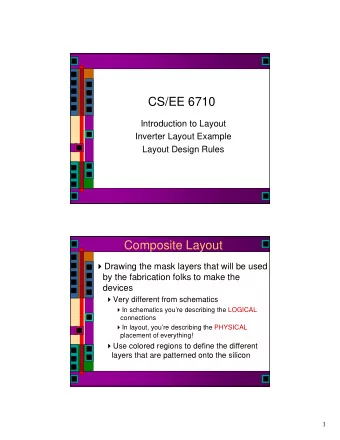
Layout and technology Dag T. Wisland Spring 2014 Outline CMOS - PowerPoint PPT Presentation
INF4420 Layout and technology Dag T. Wisland Spring 2014 Outline CMOS technology Design rules Analog layout Mismatch Spring 2014 Layout and technology 2 Introduction As circuit designers we must carefully consider how to
INF4420 Layout and technology Dag T. Wisland Spring 2014
Outline • CMOS technology • Design rules • Analog layout • Mismatch Spring 2014 Layout and technology 2
Introduction As circuit designers we must carefully consider how to draw layout for critical/sensitive parts of the circuit to get robust and predictable performance. Good simulation results from schematic is not the final answer (but necessary and a good indication). Spring 2014 Layout and technology 3
Introduction To design circuits that works as intended after manufacturing we must have a basic understanding of how circuits are manufactured, packaged, tested, and how the circuit is used (mounted on a PCB, off-chip parasitic). Spring 2014 Layout and technology 4
Physical design The physical circuit is built on a disc of silicon (wafer) layer by layer. Some layers are implanted in the substrate (front end of line), others layers stacked on top (back end of line) Spring 2014 Layout and technology 5
Physical design Layout is an encoding of the physical realization of the circuit. But not a 1:1 mapping of what we draw and what the fab puts on the masks. Spring 2014 Layout and technology 6
Photolithography Photolithography (litho) is used to transfer the layout to the physical circuit. For each layer. Light source and mask defines pattern in photoresist. Transferring the image to a physical mask on the wafer. Spring 2014 Layout and technology 7
Lithography system The layout we create is used to make a mask (or reticle) which is illuminated in the lithography system. Spring 2014 Layout and technology 8
Lithography system Photoresist hardens when exposed to light (negative resist), leaving a physical transfer of the mask on the wafer. Rest is removed. Do processing. Rinse and repeat. Spring 2014 Layout and technology 9
Lithography system Pattern on wafer is distorted by imperfections in the lithography system. Wavelength of light is a limitation for feature size. Spring 2014 Layout and technology 10
Resolution Resolution: Resolution is limited by the wavelength of light and numerical aperture DOF: (NA) of the lens (given by the angle of light captured by the lens, and NA: the refractive index, n ) Spring 2014 Layout and technology 11
Depth of focus (DOF) As the wafer is built layer by layer the geometry becomes uneven. Wafer is planarized between each step with chemical mechanical polishing (CMP) inherent tradeoff between DOF and resolution (better NA, finer pitch, more narrow DOF) Spring 2014 Layout and technology 12
Optical proximity correction (OPC), sub-resolution assist features (SRAF) Drawn shape Mask shape Spring 2014 Layout and technology 13
Spring 2014 Layout and technology 14
Extreme UV Why not use a light source with extremely short wavelength? EUV (13.5 nm) in development for a long time, still not used in large scale production. Throughput issues. Electron beam lithography (e-beam litho) possible but also throughput issues. Spring 2014 Layout and technology 15
Front end of line (FEOL) Process modules that make the active devices • Active area • Channel doping • Gate • Source/drain extension • Spacer • Junction • Silicide Spring 2014 Layout and technology 16
Back end of line (BEOL) BEOL connects the active devices using copper (Cu), separated by low- κ dielectric. • Pre-metal dielectric (PMD) • Contacts (source, drain, and gate) • Inter-level Dielectric (ILD) • Vias and metal lines Spring 2014 Layout and technology 17
Dual damascene 1. Etch trenches in the oxide (barrier). 2. Electroplating adds (excess) copper. 3. CMP to remove the excess copper. Used for via and lines. Spring 2014 Layout and technology 18
Dual damascene Why should we as designers care? Dishing affects Erosion affects wide metal lines high density lines Spring 2014 Layout and technology 19
Design rules As we have seen, the layout we draw is not perfectly reproduced on the wafer. We must comply with a set of rules to ensure that the layout we draw is manufacturable. This is a minimum requirement, and does not guarantee robust and predictable performance. Necessary but not sufficient. Spring 2014 Layout and technology 20
Design rule examples Rule name (minimum) P.1 Poly width P.2 Space poly and active P.3 Poly ext. beyond active P.4 Enc. active around gate P.5 Spc. field poly to active P.6 Spc. field poly Spring 2014 Layout and technology 21
Design rule examples Poly rules example (FreePDK45) Rule name (minimum) Length P.1 Poly width 50 nm P.2 Space poly and active 140 nm P.3 Poly extension beyond active 55 nm P.4 Enclosure active around gate 70 nm P.5 Space field poly to active 50 nm P.6 Space field poly 75 nm Spring 2014 Layout and technology 22
Design rule examples Metal1 rules example (FreePDK45) Rule name (minimum) Length M1.1 Metal1 width 65 nm M1.2 Space metal1 65 nm M1.3 Enclosure around contact (two opposite sides) 35 nm M1.4 Enclosure around via1 on two opposite sides 35 nm M1.5 Space metal1 wider than 90 nm and longer than 900 nm 90 nm M1.6 Space metal1 wider than 270 nm and longer than 300 nm 270 nm M1.7 Space metal1 wider than 500 nm and longer than 1.8 um 500nm Spring 2014 Layout and technology 23
Density design rules • Each layer must cover the chip in a specified density. • Checked inside a “moving” window, e.g. 100 µm × 100 µm. • Necessary to keep the wafer planar for imaging (DOF limitations) • Necessary to keep dishing and erosion within limits. • Automatic dummy filling to comply with density. • Must be careful with sensitive circuits. Spring 2014 Layout and technology 24
Antenna design rules Large metal area connected to a MOSFET gate collects ions during manufacturing and potentially breaks down the gate oxide (irreversibly). Spring 2014 Layout and technology 25
Design rule check (DRC) • Large number of rules, difficult to keep track of • Tool to check design rules, DRC • Foundry provides rule set as part of the PDK • Pass / fail vs. levels of severity • Default DRC rules are “minimum” • Foundry usually also provides rules for analog and sensitive circuits. Spring 2014 Layout and technology 26
Litho friendly design (LFD) • Design rules does not guarantee a robust design or good yield • Design for manufacturability (DFM) tools simulate and analyze how the layout will print • Difficult to get access to data / rules. Spring 2014 Layout and technology 27
Layout vs. schematics (LVS) • Compare layout to schematics • Make sure the layout performs the function we intended • Recognizes shapes in the layout (e.g. transistors) and how they are connected. • Foundry provides rules for recognizing devices as part of the PDK Spring 2014 Layout and technology 28
Post layout simulation Spring 2014 Layout and technology 29
Interconnect parasitics Overlap capacitance Low- κ dielectric helps reduce interconnect capacitance. Fringe capacitance also important. Spring 2014 Layout and technology 30
Interconnect parasitics Consider resistance and capacitance (and inductance). Typical metal resistance is 0.1 Ω/ □ 10 Ω per via (never use one single via) Current handling capability (electromigration) Process documentation lists actual values Spring 2014 Layout and technology 31
Interconnect parasitics Sizing metal lines is a trade-off between capacitance and resistance (and current handling capability) Wide lines, fewer squares, less resistance, but potentially more overlap capacitance. Resistance and capacitance vary due to dishing and erosion. Spring 2014 Layout and technology 32
Passive components Need passive components (resistors, capacitors) for analog and mixed signal circuits. (RF needs inductors). Process tries to minimize resistance and capacitance. Components become impractically large. Process options for passive components. Spring 2014 Layout and technology 33
Resistors Several possibilities. Need to consider: • Ω/ □ (area, practical limit for large R) • Temperature dependence (TC) • Voltage dependence (linearity) • Mismatch (ΔR/R, abs value +/ - 20 %) • Parasitic capacitance The TC and voltage dependence is not only linear, but also quadratic in the simulator. E.g. R(T) = R(T0) [1 + TC1(T - T0) + TC2(T -T0)^2]. Similar for voltage dependency. Spring 2014 Layout and technology 34
Resistors Realistic alternatives for large resistors N-well: Large R, poor TC (> 2000 ppm/C), poor linearity (< 1 %), low mismatch, parasitic capacitance from pn-depletion. Always available. Poly with silicide block: Large R, good TC (~ 100 ppm/C), reasonable linearity (< 0.1 %), low mismatch. Extra layer needed. Spring 2014 Layout and technology 35
Capacitors Need to consider • F/m^2 • Temperature dependence (TC) • Voltage dependence (linearity) • Mismatch (ΔR/R) • Cost Spring 2014 Layout and technology 36
Capacitors MOSCAP, using gate capacitance as a capacitor. Very high capacitance per unit area, non-linear, useful for decoupling, but gate leakage current is problematic. PiP (poly-insulator-poly), using two poly layers. Usually not available in modern CMOS. Spring 2014 Layout and technology 37
Capacitors Spring 2014 Layout and technology 38
Recommend
More recommend
Explore More Topics
Stay informed with curated content and fresh updates.
