ITRPV 9 th edition 2018 - report release and key findings Markus - PowerPoint PPT Presentation
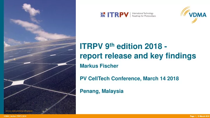
ITRPV 9 th edition 2018 - report release and key findings Markus Fischer PV CellTech Conference, March 14 2018 Penang, Malaysia Source: www.siemens.com/presse VDMA | Author ITRPV 2018 Page 1 | 13 March 2018 Page 1 | 15 March 2017 Outline
ITRPV 9 th edition 2018 - report release and key findings Markus Fischer PV CellTech Conference, March 14 2018 Penang, Malaysia Source: www.siemens.com/presse VDMA | Author ITRPV 2018 Page 1 | 13 March 2018 Page 1 | 15 March 2017
Outline 1. ITRPV Introduction 2. PV Learning Curve and Cost Considerations ITRPV – Results 2017 3. - Wafer - Materials, Processes, Products - Cell - Materials, Processes, Products - Module - Materials, Processes, Products - Systems 4. Summary and Outlook VDMA | Author ITRPV 2018 Page 2 | 13 March 2018
Outline 1. ITRPV Introduction 2. PV Learning Curve and Cost Considerations ITRPV – Results 2017 3. - Wafer - Materials, Processes, Products - Cell - Materials, Processes, Products - Module - Materials, Processes, Products - Systems 4. Summary and Outlook VDMA | Author ITRPV 2018 Page 3 | 13 March 2018
ITRPV – Methodology Working group today includes 55 contributors from Asia, Australia, Europe, and US SILICON CRYSTAL. WAFER CELL MODULE SYSTEM Participating Independent data Review of data Next companies collection / processing Preparation of publication ITRPV by VDMA regional chairs edition Chairs US Chairs PRC Chairs TW Chairs US Photovoltaic Equipment Parameters in main areas are discussed Diagrams of median values | Author ITRPV 2018 VDMA Page 4 | 13 March 2018
Review ITRPV predictions Finger width 140 Contributors: 55 (40) 120 100 Figures: 71 (60) 80 µm Materials: 16 (14) 60 ITRPV 2018 Processes: 21 (18) 40 Products: 14 (12) 20 PV systems: 8 (7) 0 20092010201120122013201420152016201720182019202020212022202320242025202620272028 1. Edition 2. Edition 3. Edition 4. Edition 5. Edition 6. Edition 7. Edition 8. Edition 9. Edition Review ITRPV predictions Prediction quality since 2009: Wafer thickness (mono) 200 well predicted and realized Finger width trend 180 (Front side improvement is key for: 160 140 1. Silver reduction (world market driven Silver price) 120 2. performance increase µm 100 80 bad predicted and no progress Wafer thickness trend ITRPV 2018 60 40 Mono shows indication of reduction 20 (Poly-Si depends on PV market development) 0 20092010 2011 2012 2013 2014 2015 2016 2017 2018 2019 202020212022 2023 2024 2025 2026 2027 2028 1. Edition 2. Edition 3. Edition 4. Edition 5. Edition 6. Edition 7. Edition 8. Edition 9. Edition VDMA | Author ITRPV 2018 Page 5 | 13 March 2018
Outline 1. ITRPV Introduction 2. PV Learning Curve and Cost Considerations ITRPV – Results 2017 3. - Wafer - Materials, Processes, Products - Cell - Materials, Processes, Products - Module - Materials, Processes, Products - Systems 4. Summary and Outlook VDMA | Author ITRPV 2018 Page 6 | 13 March 2018
PV learning curve Shipments /avg. price at years end: Learning curve for module price as a function of cumulative shipments 2016: 76 GWp / 0.37 US$/Wp 2017: 105 GWp / 0.34 US$/Wp ITRPV 2018 ≈ 414 GWp o/a shipment: ≈ 402 GWp o/a installation: 400 GWp milestone passed! more than doubling since 2014 2015 LR 22.8% (1976 …. 2017) 12 / 2017 400 GWp moderate price reduction @ impressive volume VDMA | Author ITRPV 2018 Page 7 | 13 March 2018
Cost consideration 1.59 US$ Price Trend for c-Si modules 0.58 US$ 1,8 1,7 Module Module 25% Module 0.34 US$ 1,6 37% 42% ITRPV 2018 1,5 Cell 20% 1,4 Cell 22% Cell 23% 1,3 Wafer 29% Spot Pricing [USD/Wp] 1,2 Wafer 18% Wafer 23% 1,1 Poly Si 26% Poly Si 23% 1,0 Poly Si 12% reduction 01/2011 01/2016: ≈ 64 % 0,9 01_2011 01_2016 12_2017 0,8 reduction 01/2016 12/2017: ≈ 42 % 0,7 0,6 (reduction 01/2017 12/2017: ≈ 8 %) 0,5 0,4 Moderate price reduction due to China demand 0,3 0,2 risk of overheating in 2018 0,1 0,0 01.2011 01.2012 01.2013 01.2014 01.2015 01.2016 01.2017 01.2018 c-Si-wafer share still at 40% Silicon Multi Wafer Multi Cell Multi Module Cost pressure on module remains VDMA | Author ITRPV 2018 Page 8 | 13 March 2018
Outline 1. ITRPV Introduction 2. PV Learning Curve and Cost Considerations ITRPV – Results 2017 3. - Wafer - Materials, Processes, Products - Cell - Materials, Processes, Products - Module - Materials, Processes, Products - Systems 4. Summary and Outlook VDMA | Author ITRPV 2018 Page 9 | 13 March 2018
Wafer: wafering technology (1) Trend: wafering technology for mono-Si Trend: wafering technology for mc-Si 100% 100% 90% 90% 80% 80% 70% 70% 60% 60% 50% 50% 40% 40% 30% 30% ITRPV 2018 ITRPV 2018 20% 20% 10% 10% 0% 0% 2017 2018 2020 2022 2025 2028 2017 2018 2020 2022 2025 2028 slurry based electroplated diamonds resin bond diamonds slurry based electroplated diamonds resin bond diamonds Slurry based wafering will fast disappear also for mc-Si DWS replaced slurry nearly completely main challenge: texturing Electroplated diamond wire is mostly used VDMA | Author ITRPV 2018 Page 10 | 13 March 2018
Wafer: wafering technology (2) Trend: Kerf loss / TTV Trend: throughput crystallization/ wafering 150% 140 140% ITRPV 2018 120 130% Kerf D 40µm 100 120% D 60µm 110% 80 [µm] ITRPV 2018 100% 60 90% 2017 2018 2020 2022 2025 2028 40 crystal growth per tool (mc-Si) slurry based wire sawing relative troughput CCz[kg/h]/Cz(kg/h] diamond wire based 20 1.400 ITRPV 2018 0 1.200 2017 2018 2020 2022 2025 2028 Kerf loss for slurry based wire sawing Kerf loss for diamond wire sawing 1.000 TTV for slurry based wire sawing TTV for diamond wire sawing 800 Gen 8 [kg] Gen 7 600 diamond wire sawing advantage : Gen 6 400 realizing fast, significant kerf reduction 200 No big change in thickness variation is expected 0 2017 2018 2020 2022 2025 2028 mc-Si mono-Si continued throughput improvement in crystallization/wafering VDMA | Author ITRPV 2018 Page 11 | 13 March 2018
Wafer: Materials - poly-Si utilization Trend: poly-Si consumption for c-Si wafers 20 poly Si utilization: standard wafer ≈ 10g 19 18 slurry based wafering: 200% - 17 DWS 160% - 16 [gram] 15 14 Reduced kerf loss enables big reduction ITRPV 2018 13 Mono / mc-Si show slight difference 12 11 Thickness reduction will enable further reduction 10 2017 2018 2020 2022 2025 2028 mc-Si, slurry based mono-Si, slurry based mc-Si, diamond wire based mono-Si, diamond wire based VDMA | Author ITRPV 2018 Page 12 | 13 March 2018
Wafer: Product – wafer thickness trend • Still no progress in mc-Si thickness reduction • Median mono: decreased in 2017! Wafer thickness [µm] 190 190 180 180 170 170 160 150 160 140 130 150 120 [µm] 2009 2015 2017 110 140 100 1st 2nd 3rd 4th 5th 6th 7th 8th 9th 130 ITRPV Edition 120 ITRPV 2018 180µm = preferred thickness since 2009 110 100 • Thickness reduction obviously started for Mono 90 cost reduction potential 2017 2018 2020 2022 2025 2028 diamond wire will support Wafer thickness multi Wafer thickness mono limit of cell thickness in future modul technology New module technologies ready! VDMA | Author ITRPV 2018 Page 13 | 13 March 2018
Wafer: Product - market share of material types Trend: share of c-Si material types 100% n-type casted-Si domination may be not for ever: 90% ITRPV 2018 p-type mono dominates market in 2017 (60%) 80% • Casting technology: 70% IHS Markit data standardp-type mc-Si disappears fast 60% no “ come back” of mono -like expected 50% • Mono technology gains market: 40% p-type mc n-type material share will increase 30% n- + p-type market share today ≈ 40% 20% 10% • p-type material is expected to stay dominant 0% IHS 2017 2017 2018 2020 2022 2025 2028 mainly due to solved degradation challenge p-type mc p-type HPmc p-type monolike p-type mono n-type mono Mono share is expected to increase (driven by n-type) • 2017 values in line w/ IHS analysis VDMA | Author ITRPV 2018 Page 14 | 13 March 2018
Wafer: Product – market share of different wafer formats Trend: wafer mono-Si Trend: wafer dimension mc-Si 100% 100% 90% 90% 80% 80% 70% 70% 60% 60% 50% 50% 40% 40% ITRPV 2018 ITRPV 2018 30% 30% 20% 20% 10% 10% 0% 0% 2017 2018 2020 2022 2025 2028 2017 2018 2020 2022 2025 2028 156.0 +-0.5 * 156.0 +- 0.5 mm² 156.75 +-0.25 * 156.75 +- 0.25 mm² 156.0 +-0.5 * 156.0 +- 0.5 mm² 156.75 +-0.25 * 156.75 +- 0.25 mm² 161.75 +-0.25 * 161.75 +- 0.25 mm² 161.75 +-0.25 * 161.75 +- 0.25 mm² Very fast transition to new formats for mono and mc-Si 156.75 x 156.75 mm² is mainstream today! 161.75 x 161.75 mm² is expected in future further changes depend on module dimensions VDMA | Author ITRPV 2017 | Author ITRPV 2018 Page 15 | Page 15 | 13 March 2018
Outline 1. ITRPV Introduction 2. PV Learning Curve and Cost Considerations ITRPV – Results 2017 3. - Wafer - Materials, Processes, Products - Cell - Materials, Processes, Products - Module - Materials, Processes, Products - Systems 4. Summary and Outlook VDMA | Author ITRPV 2018 Page 16 | 13 March 2018
Recommend
More recommend
Explore More Topics
Stay informed with curated content and fresh updates.
