Introduction When the characteristic length of the objective is - PowerPoint PPT Presentation
Characterization and design of micro-photonic devices and optical metamaterial with full wave simulations Sy-Bor Wen, Arun Bhaskar, Vijay M. Sundaram Department of Mechanical Engineering, Texas A&M University, College Station, TX 77843
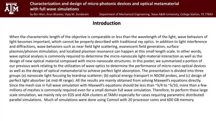
Characterization and design of micro-photonic devices and optical metamaterial with full wave simulations Sy-Bor Wen, Arun Bhaskar, Vijay M. Sundaram Department of Mechanical Engineering, Texas A&M University, College Station, TX 77843 Introduction When the characteristic length of the objective is comparable or less than the wavelength of the light, wave behaviors of light becomes important, which cannot be properly described with traditional ray optics. In addition to light interference and diffractions, wave behaviors such as near field light scattering, evanescent field generation, surface plasmon/phonon stimulation, and localized plasmon resonance can happen at this small length scale. In other words, wave optical analysis is commonly required to determine the micro-nanoscale light-material interaction as well as the design of new optical material composed with micro-nanoscale structures. In this poster, we summarized a portion of our previous work relating to the utilization of wave optics to determine the performance of micro-nano optical devices as well as the design of optical metamaterial to achieve perfect light absorption. The presentation is divided into three groups (a) nanoscale light focusing by teardrop scatterer; (b) optical energy transport in NSOM probes, and (c) design of perfect light absorber (at mid- IR range). All the results are mainly obtained from solving Maxwell’s equations directly. Since the mesh size in full wave simulation with Maxwell’s equations should be less than ~λ/4 to ~λ/10, more than a few millions of meshes is commonly required even for a small domain full wave simulation. Therefore, to perform these large scale simulation, we mainly rely on EOS and ADA clusters at TAMU especially for cases requiring parametric distributed parallel simulations. Much of simulations were done using Comsol with 20 processor cores and 600 GB memory.
Characterization and design of micro-photonic devices and optical metamaterial with full wave simulations Sy-Bor Wen, Arun Bhaskar, Vijay M. Sundaram Department of Mechanical Engineering, Texas A&M University, College Station, TX 77843 Theory The numerical results presented in the following sections are based on solving the following two governing equations under 2D evolutionally symmetric or 3D conditions with either finite different finite element method (FEM). (a) Wave optical simulation with Maxwell’s equations in frequency domain 𝛼 ∙ 𝐸 = 0 ; 𝛼 ∙ 𝐶 = 0 ; 𝛼 × 𝐹 = −𝑘𝜕𝜈 0 𝐼 ; 𝛼 × 𝐼 = −𝑘𝜕𝜁 𝑠0 𝜁 0 𝐹 where 𝐹 , 𝐸 , 𝐶 and 𝐼 are the electric field, electric displacement, magnetic induction and magnetic field in the frequency domains; 𝜁 𝑠 is the relative permittivity of the material, 𝜁 0 is the permittivity of free space; 𝜈 0 is the permeability of the material. The induced current density is 𝐾 = 𝑘𝜕𝐸 . The time average joule heating 𝜒 is ½Re( −𝑘𝜕𝐹 ∙ 𝐸 ∗ ) . (b) Heat transfer simulation with two temperature model for the heat diffusion in the solid 𝜖𝑈 𝐷 𝑞 𝜖𝑈 𝐷 𝑓 𝑞 𝑓 𝐷 𝑓 𝜖𝑢 = 𝜒 + 𝛼 ∙ 𝐿 𝑓 𝛼𝑈 𝑓 − 𝜐 𝑓−𝑞 (𝑈 𝑓 − 𝑈 𝑞 ) 𝐷 𝑞 𝜖𝑢 = 𝜒 + 𝛼 ∙ 𝐿 𝑞 𝛼𝑈 𝑞 − 𝜐 𝑓−𝑞 (𝑈 𝑓 − 𝑈 𝑞 ) where 𝐷 𝑓 and 𝐷 𝑞 are the heat capacity of electrons and phonons, respectively; 𝑈 𝑓 and 𝑈 𝑞 are the electron and phonon temperatures, respectively; 𝐿 𝑓 and 𝐿 𝑞 are electron and phonon conductivity, respectively; and 𝜐 𝑓−𝑞 is the relaxation time between the electrons and phonons. To reduce the simulation time, the wave optics simulation is decoupled with the heat transfer analysis, which is a good assumption when the light pulse width is much less than the thermal diffusion time constant.
Characterization and design of micro-photonic devices and optical metamaterial with full wave simulations Sy-Bor Wen, Arun Bhaskar, Vijay M. Sundaram Department of Mechanical Engineering, Texas A&M University, College Station, TX 77843 Nanometer focusing by teardrop scatterer Most of micro-nano optical devices require metal structures to confine light to a nm spot through evanescent wave generation and/or stimulation of surface/localized plasmon resonance. However, metal structure can cause joule heating which can easily damage the optical device under high energy operation. Therefore, we decided to design a new type of nano- optical device which can focus light to a deep nanoscale spot purely with dielectric components. The approach we developed is based on of cascade light focusing (figure 1): with an appropriate ball lens placed at the end of the optical fiber, the light emitted from the optical fiber can be confiner to a spot ~λ with λ the light wavelength (figure 1a). To reduce a light spot to Figure 1: Schematic of deep nm light focusing with cascade light focusing ~λ/ 2, a microsphere with a diameter around 5-10 λ can be placed at the through (a) a ball lens, then (b) a microsphere, and then (c) a teardrop focal spot of the ball lens to induced the photonic jet effect (figure 1b). scatterer. The final pure dielectric optical device is illustrated in (d). Figure 2 shows the combination of a 58 μm ball lens and a 3 μm microsphere at the focal spot of the ball lens to compress the light from a 10 μm core optical fiber to a ~250 nm spot when λ~ 400 nm. To further reduce the light spot to sub 100 nm spot, we proposed to place a teardrop scatterer at the photonic jet after the microsphere (figure 1c). The teardrop scatter can be considered as a snowman scatterer (figure 3a) with a filled gap between the top and bottom spheres (figure 3b). The resulting cascade light focusing device as a combination of a ball lens, a microsphere and a teardrop scatterer stacked on the top of a cleaved optical fiber is illustrated in figure 1d. Figure 2: Assembly of a 58 μ m ball lens and a 3 µm microsphere at its focal spot to confine the 400 nm light to a ~250 nm spot.
Characterization and design of micro-photonic devices and optical metamaterial with full wave simulations Sy-Bor Wen, Arun Bhaskar, Vijay M. Sundaram Department of Mechanical Engineering, Texas A&M University, College Station, TX 77843 Nanometer focusing by teardrop scatterer When both the top and bottom spheres of the teardrop scatterer are made with silica with diameters equal to 500 nm and 10 nm, respectively, we figured out that cascade light focusing can provide a ~5 nm spot at the end of the teardrop scatterer with high local electric field intensity (figure 4). The simulation was conducted with EOS cluster of the TAMU. Each simulation takes about ~800 BU. Figure 4: full wave simulation results of ~5 nm light confinement Figure 3: Schematic of a (a) snowman scatterer, and (b) a at the forward end of the teardrop scatterer teardrop scatterer used to confine light to a deep nm spot Sundaram, V. M, Wen, S. B. “Nanoscale high intensity light focusing with pure dielectric non-spherical scatterer ,” Optics Letters. 39, 2014
Characterization and design of micro-photonic devices and optical metamaterial with full wave simulations Sy-Bor Wen, Arun Bhaskar, Vijay M. Sundaram Department of Mechanical Engineering, Texas A&M University, College Station, TX 77843 Optical energy transport in NSOM probes Near field scanning optical microscopy (NSOM), which is broadly utilized in nanoscale detection and analysis, has the ability to break the diffraction limit of light and achieve a spatial resolution down to tens of nm through multiple internal reflections and the associated generation of evanescent waves (figure 5). In traditional NSOM applications, the light intensity conveyed by a NSOM system is limited to a relatively low energy level to prevent damage to the target and to the NSOM probe. Therefore, in most applications relating to NSOM, the heating of the target is small. Recently, people start using NSOM to deliver intense laser pulse to a semi-conductor or metal surface to achieved nm level direct laser machining. Figure 6 shows some experimental results we obtained by coupling a 50 nm apertured NSOM probe with 100 fs laser pulse at λ= 400 nm Figure 5. Side view of a NSOM probe with light Figure 6. Nano-patterns generated on silicon using femtosecond laser (a) before etching emitting from the tip at the left end. with BHF (b) after etching with BHF (c) after single pulse (d) after 200 laser pulses.
Characterization and design of micro-photonic devices and optical metamaterial with full wave simulations Sy-Bor Wen, Arun Bhaskar, Vijay M. Sundaram Department of Mechanical Engineering, Texas A&M University, College Station, TX 77843 Optical energy transport in NSOM probes Figure 7: Spatial For these nm direct laser distribution of the electric machining with NSOM, due to the field in the (a) polarization higher input laser energy, NSOM probe can easily be damaged due direction, (b) normal to the to high temperature melting polarization direction, and and/or exfoliation of the metal (c) end surface of the coating on the NSOM probe. To NSOM probe during a 100 better understand the heating in fs laser pulse at 400 nm. NSOM probes in order to control it The entire simulation in the nm direct laser machining, domain is illustrated in (d). we have performed full wave simulation to study the light transport in the NSOM probe and the associated heating process. Figure 7 shows the simulated electric field distribution in an NSOM probe under a HE11 mode light illumination
Recommend
More recommend
Explore More Topics
Stay informed with curated content and fresh updates.


