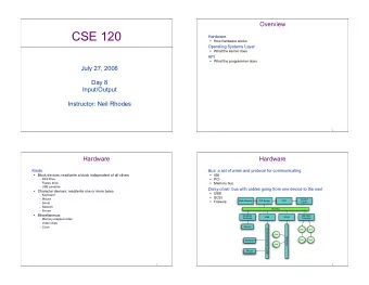
Hardware MSP430F1611 Ports: P1-P6 Each port == 8 pins Memory, - PowerPoint PPT Presentation
Hardware MSP430F1611 Ports: P1-P6 Each port == 8 pins Memory, clock RAM: between 256 and 16K bytes, depending on the model Code (flash == EEPROM): from 8KB to 256KB Max clock rate up to 25MHz Memory layout Port access These ones can
Hardware
MSP430F1611 Ports: P1-P6 Each port == 8 pins
Memory, clock RAM: between 256 and 16K bytes, depending on the model Code (flash == EEPROM): from 8KB to 256KB Max clock rate up to 25MHz
Memory layout
Port access These ones can trigger interrupts
Sensor interfaces 2 UARTs, each reconfigurable into: SPI I 2 C direct pin access ADC (8 ports usable for this purpose) DAC (2 ports) – for actuators
UART Two ways (separate wires) Tx/Rx Digital signal (two levels) assuming: limited length of a data unit (byte) both parties know the fixed duration of a bit high low start 1 1 1 0 1 1 0 0 stop
SPI The primary difference: clock is provided on a separate wire it works both ways at once (sort of) CLK OUT IN
SPI timing
SPI implementation Master SOMI Slave b7 b7 There are two byte-sized shift registers interconnected by the two data lines. A transfer always involves exchanging their contents (so it is always both ways). b0 b0 SIMO CLK
I 2 C Serial DAta Serial CLock
Example: SHT7x
Connection
Protocol
Even simpler Temperature sensor Single-wire interface, i.e., no clock!
Connecting
Communication (startup)
Communication (read/write)
Device identification protocol Command “search ROM” 0xF0 All devices respond with subsequent bits of their IDs (64 of them), each bit being reported twice positive + negated. The micro responds after every bit with 0 or 1 selecting the subset of devices that it wants to continue with. The remaining ones remain silent until the next reset pulse. 00 – there are devices with both 0 and 1 on this position 01 – all devices have 0 on this position 10 – all devices have 1 on this position
ADC (MSP430) Up to 8 configurable pins (independent inputs) 12-bit accuracy: d = 4096 x (V - V ref- ) / (V ref+ - V ref- ) reference measured lower bound upper bound Can be sampled automatically at prescribed rate
Example PAR V ref+ = 1.2V (Zener) V ref- = 0 c = f x d f = 1200x5/4096 f = 1.465
Recommend
More recommend
Explore More Topics
Stay informed with curated content and fresh updates.


