for the IBL Detector Andrea Gaudiello Universit degli Studi Di - PowerPoint PPT Presentation
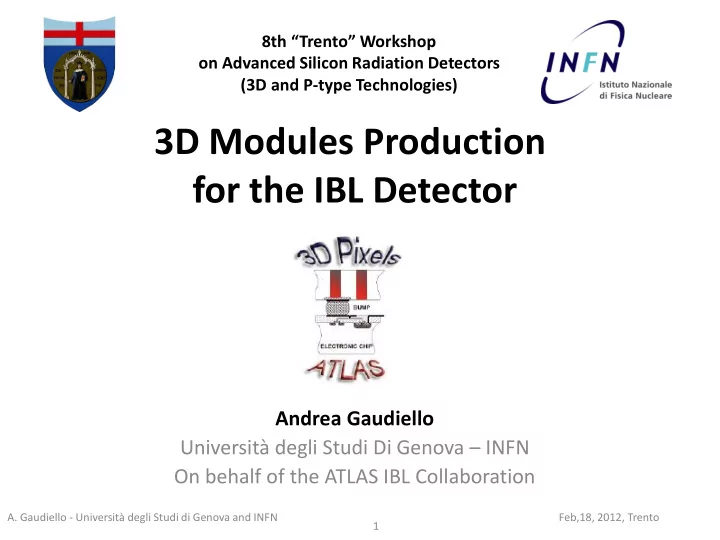
8th Trento Workshop on Advanced Silicon Radiation Detectors (3D and P-type Technologies) 3D Modules Production for the IBL Detector Andrea Gaudiello Universit degli Studi Di Genova INFN On behalf of the ATLAS IBL Collaboration A.
8th “Trento” Workshop on Advanced Silicon Radiation Detectors (3D and P-type Technologies) 3D Modules Production for the IBL Detector Andrea Gaudiello Università degli Studi Di Genova – INFN On behalf of the ATLAS IBL Collaboration A. Gaudiello - Università degli Studi di Genova and INFN Feb,18, 2012, Trento 1
Outline Production Sensor Production Modules Production Bump-Bonding Problems Comparison Breakdown CNM and FBK sensors BARE Sensor Changes after Assembly V Breakdown comparation after the assembly Noise Vs HV Source Scan and Time of Threshold (ToT) A. Gaudiello - Università degli Studi di Genova and INFN Feb,18, 2012, Trento 2
Staves 3D Sensors 3D Sensors A stave is equipped with: Central region: 12 Double-chip modules (Planar/CiS) Forwarded regions: 4+4 Single-chip modules (3D FBK & CNM) The Insertable B-Layer (IBL) is composed by 14 Staves A total of 112 3D Modules are in the IBL A. Gaudiello - Università degli Studi di Genova and INFN Feb,18, 2012, Trento 3
Summary of Production 3D Wafers Wafer Produced & Selected UBM Comment Tasted (by IZM) FBK – A10 20 12 12 FBK – A11 22 4 4 FBK – A12 17 11+( 2 broken) 10 2 broken in shipping FBK – A13 11 4 - Values and table from G. Darbo CNM1 18+1 16 16+1 18 wafer data sheets CNM2 17 12 9 17 wafer data sheets CNM3 15 12 TOTAL: 121 71+(2 broken) 51+1 1 with 2 good tiles CNM FBK Produced & tested wafers 51 70 Selected wafers 40 31 UBMed wafers 26 26 Green tiles on Selected 203 + 13 (broken) 135 Tot: 250 Green tiles with UBM 133 117 Feb,18, 2012, Trento 4 A. Gaudiello - Università degli Studi di Genova and INFN
Sensors Population Comparison between FBK and CNM V-Breakdown on Wafer (BARE) (Type A – Good Quality) A. Gaudiello - Università degli Studi di Feb,18, 2012, Trento 5 Genova and INFN
Sensors Population Comparison between FBK and CNM Ileak on Wafer (BARE) (Type A – Good Quality) CNM: Ileak current is measured only on the Guard Ring A. Gaudiello - Università degli Studi di Feb,18, 2012, Trento 6 Genova and INFN
Building and Qualification of Modules Sensors are flip-chipped at IZM and then delivered to Genova and Bonn for module assembly and testing. Assembly of a module starts with gluing a module pigtail on bare module (SC/DC). Wirebondings are done to the FE pads, to the HV and to the test pads. It is also done a pull test to qualify the quality. Module is tested with USBPix readout system A. Gaudiello - Università degli Studi di Feb,18, 2012, Trento 7 Genova and INFN
Building and Qualification of Modules The qualification of modules consists of four types of tests: INIT: Very preliminary electrical test after assembly to test that all the wire-bonds and connection are properly done. ASSY: Electrical test at ambient temperature, in which is checked the proper basic functioning of the module (e.g. IV Curve, bumps connectivity). Also done the Tuning at working point of 3k 𝑓 − Threshold and 9BC @ 20k 𝑓 − . BURN: Module is thermal cycling (-40, +40 °C for 2-3 days) and retested at ambient temperature with the same test of ASSY. FLEX: Complete calibration of a module. All tests are executed at ~ − 10°𝐷 . A. Gaudiello - Università degli Studi di Feb,18, 2012, Trento 8 Genova and INFN
Bump-Bonding Problems In the first three batches of bump-bonding were assembled a total of 85 Modules: 67 DC and 18 SC (139 DC and 124 SC flip chipped). We have observed in ~80% of Modules two kinds of bump defects/damage: • Unconnected bumps (‘ opens ’): Small Rate ~20%, Observed ‘ islands ’ of unconnected bumps This is probably attributed to the flip chip process • Single bumps defects distribuited over the modules (‘shorts’): High Rate ~80%, shorted pixel The reason of this problem is not completely understood but results suggests flip chip, in particular large amount of flux left between bumps. Feb,18, 2012, Trento 9 A. Gaudiello - Università degli Studi di Genova and INFN
Bump-Bonding Problems Images by F.Hügging CNM5860-23-03_sensor_center_flux particle_not connected_200x Too much flux during the flip chip could be the cause of the open bumps. Solution: IZM changed the flip chip process (glycerin as tacking media is used) and uses a different bonder (Panasonic FCB3) In the last batch (4) this problem has been resolved! Quality and yield is very good: All 9 DC and 16 SC batch 4 modules tested good No bump bonding problems (shorts and opens) Feb,18, 2012, Trento 10 A. Gaudiello - Università degli Studi di Genova and INFN
Bump-Bonding Problems Example of unconnected bumps (Module 37-23-03) Images by F.Hügging Threshold Noise Feb,18, 2012, Trento 11 A. Gaudiello - Università degli Studi di Genova and INFN
Bump-Bonding Problems Example of single bump defects (Module 94-25-01) Reference: C.Gemme and F.Hügging (ATLAS) Threshold Am241 - Occupancy Cross-Talk with HV Feb,18, 2012, Trento 12 A. Gaudiello - Università degli Studi di Genova and INFN
Summary of Production Modules Double Chip Module Production (Bonn and Genova) Plot by F. Hügging, Image by G.Darbo A. Gaudiello - Università degli Studi di Feb,18, 2012, Trento 13 Genova and INFN
Summary of Production Modules Single Chip Module Production (Bonn and Genova) Plot by F. Hügging, Image by G.Darbo A. Gaudiello - Università degli Studi di Feb,18, 2012, Trento 14 Genova and INFN
Examples of IV Curve CNM FBK 2𝜈𝐵 2𝜈𝐵 A. Gaudiello - Università degli Studi di Feb,18, 2012, Trento 15 Genova and INFN
Sensors V Breakdown Changes after the Assembly (FBK Modules) Measured on Module Measured on Wafer Type C: Bad Quality Sensor Type A: Good Quality Sensor A. Gaudiello - Università degli Studi di Feb,18, 2012, Trento 16 Genova and INFN
Sensors V Breakdown Changes after the Assembly (CNM Modules) Measured on Module Measured on Wafer Type C: Bad Quality Sensor Type A: Good Quality Sensor A. Gaudiello - Università degli Studi di Feb,18, 2012, Trento 17 Genova and INFN
Noise VS High Voltage CNM (60-03-06) 160 𝒇 − 320 𝒇 − Noise - High Voltage On Noise - High Voltage Off A. Gaudiello - Università degli Studi di Feb,18, 2012, Trento 18 Genova and INFN
Noise VS High Voltage FBK (12-08-05) 144 𝒇 − 210 𝒇 − Noise - High Voltage On Noise - High Voltage Off A. Gaudiello - Università degli Studi di Feb,18, 2012, Trento 19 Genova and INFN
Noise VS High Voltage FBK (12-02-08) Disconnected Bumps Disconnected Bumps 150 𝒇 − 235 𝒇 − Noise - High Voltage On Noise - High Voltage Off The cut on D -noise HV on/off has to be tuned independently for CNM and FBK when more statistics will be available 20
Noise VS High Voltage Here is checked on few samples the expected dependence of Noise Vs HV. CNM FBK Operation working point at -20V A. Gaudiello - Università degli Studi di Feb,18, 2012, Trento 21 Genova and INFN
Source Scan Occupancy (Am - 241) CNM FBK Shadows of the SMDs components and LV test pins are clearly visible. Occupancy of FBK rows and columns edge (barely visible in the right plot) is larger due to lateral depletion in the fence region. A. Gaudiello - Università degli Studi di Feb,18, 2012, Trento 22 Genova and INFN
Source Scan and Time of Threshold (ToT) Comparison between FBK and CNM ToT in Source Scan, Cluster and Hit Source: Americium 241 CNM FBK Clusters Clusters Single Hits Single Hits Preliminary Test Comparison ToT Cluster Vs ToT Hit CLUSTER SIZE A. Gaudiello - Università degli Studi di Feb,18, 2012, Trento 23 Genova and INFN
Source Scan and Time of Threshold (ToT) Comparison between FBK and CNM ToT in Source Scan, Cluster and Hit Source: Strontium 90 CNM FBK Clusters Clusters Single Hit Single Hit Preliminary Test Comparison ToT Cluster Vs ToT Hit CLUSTER SIZE A. Gaudiello - Università degli Studi di Feb,18, 2012, Trento 24 Genova and INFN
The module production has just restarted after problems encountered at IZM. Waiting for more statistics to produce systematics distributions for FBK and CNM. Thank You! A. Gaudiello - Università degli Studi di Feb,18, 2012, Trento 25 Genova and INFN
Sensors Population Comparison between FBK and CNM Ileak on Wafer (BARE) FBK CNM Guard ring CNM:The Ileak current is During the Ileak measure measured only on the all pixels are connected guard ring A. Gaudiello - Università degli Studi di Feb,18, 2012, Trento 26 Genova and INFN
Noise VS High Voltage For 3D modules (especially CNM) solely Δnoise can not identify open bumps. CNM FBK From M. Backhaus A. Gaudiello - Università degli Studi di Feb,18, 2012, Trento 27 Genova and INFN
Source Scan and Time of Threshold (ToT) Comparison between FBK and CNM ToT in Source Scan, Cluster and Single Pixel Source: Americium 241 Central Columns - All Column 0 Central Columns (39-42) Module CNM CLUSTER SIZE A. Gaudiello - Università degli Studi di Feb,18, 2012, Trento 28 Genova and INFN
Source Scan and Time of Threshold (ToT) Comparison between FBK and CNM ToT in Source Scan, Cluster and Single Pixel Source: Strontium 90 Column 0 Central Columns (39-42) FBK CLUSTER SIZE A. Gaudiello - Università degli Studi di Feb,18, 2012, Trento 29 Genova and INFN
Recommend
More recommend
Explore More Topics
Stay informed with curated content and fresh updates.
