FABRICATION OF SI QUANTUM-DOT SOLAR CELL AND ITS CURRENT-VOLTAGE - PowerPoint PPT Presentation
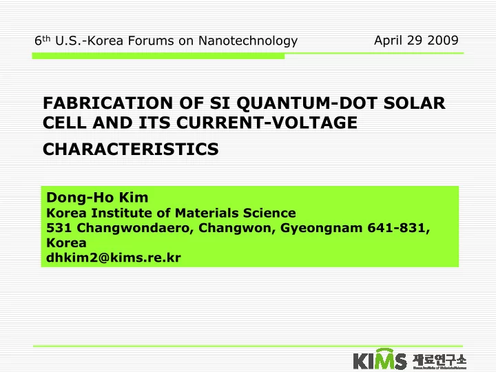
6 th U.S.-Korea Forums on Nanotechnology April 29 2009 FABRICATION OF SI QUANTUM-DOT SOLAR CELL AND ITS CURRENT-VOLTAGE CHARACTERISTICS Dong-Ho Kim Korea Institute of Materials Science 531 Changwondaero, Changwon, Gyeongnam 641-831, Korea
6 th U.S.-Korea Forums on Nanotechnology April 29 2009 FABRICATION OF SI QUANTUM-DOT SOLAR CELL AND ITS CURRENT-VOLTAGE CHARACTERISTICS Dong-Ho Kim Korea Institute of Materials Science 531 Changwondaero, Changwon, Gyeongnam 641-831, Korea dhkim2@kims.re.kr
Introduction � All-Si tandem solar cell Inexpensive Si thin-film technology in combination � with high efficiency multi-bandgap approach. Si QD superlattices are used as the higher bandgap � cells in a tandem stack
Device fabrications � Si QD layers SRO(4nm)/SiO 2 (2nm) � High T annealing � � Interdigitated structure Photolitho and RIE � E.-C. Cho, et.al, Nanotechnology 19 , 245201 (2008). Al electrodes �
Photovoltaic behaviors J D : dark IV J: light IV (AM1.5G spectrum, 25 o C) superposition approximation (J(V) = J D (V) − Jsc) does not hold PV characteristic properties of a prototype cell � Effective area : 4.7 mm 2 � Voc = 394 mV, Jsc = 62 µ A/cm 2 � Voltage–dependent photocurrent collection � Our Si QD layers in dielectric matrix have lots of defects � diffusion length would be very, very short �
Current-Voltage characterization Applying a diode model to 1000 � y = 7.640E-02x + 9.807E+01 dark IV data 800 R 2 = 9.999E-01 dV/dJ ( Ω -cm 2 ) 600 = × + J (V) J [exp(q/nkT V ) - 1] V /R D 0 j j sh 400 where, V j =V − J × R s 200 0 Determination of parameters � 0.E+00 5.E+03 1.E+04 (a) 1/J (cm 2 /A) n, J 0 , R s , R sh � 1.E-02 Experimental and fitted dark � J (experimental) 1.E-03 J (fitted) I-V curves J (A/cm 2 ) 1.E-04 1.E-05 1.E-06 J shunt J diode 1.E-07 0 0.2 0.4 0.6 0.8 1 (b) (V)
Current-Voltage characterization In reverse bias � 1.E-05 (V) This poor rectifying behaviour � 0.E+00 of Si QD pn-junction is due to -1 -0.8 -0.6 -0.4 -0.2 0 0.2 the inter-diffusion of dopants -1.E-05 J shunt J (A/cm 2 ) J D (experimental) -2.E-05 (c) -3.E-05 Photocurrent J L (V)=J D (V)-J(V) � 1.5E-04 Tunneling probabilities of J L (A/cm 2 ) � photogenerated carriers in QD 1.0E-04 increase with electric field 5.0E-05 Conduction mechanism in QD � (V) materials is still complex issue 0.0E+00 -1 -0.8 -0.6 -0.4 -0.2 0 0.2 0.4 0.6 (d) -5.0E-05
Concluding remarks A single junction Si QD solar cell was fabricated and its � photovoltaic properties were examined. The prototype device is promising towards the realization of � all-silicon tandem solar cells based on Si QD materials For practical usage as a top cell in tandem device, � Voc should be increased above that of the standard cystalline Si solar cells (>700 mV) and the current be improved in orders of magnitude Acknowledgements � Thank 3rd Gen members in Photovoltaics Centre of Excellence in � Univ. New South Wales (AU) Korea Research Foundation Grant funded by the Korean � Government (MOEHRD) (KRF-2007-611- D00015). Korea Nano Technology Research Association �
Recommend
More recommend
Explore More Topics
Stay informed with curated content and fresh updates.
