Electron Spectrometers Scanning Probe Microscopy Sources LEEM/PEEM - PDF document
SPECS is specialized in the development and production of customized UHV surface analysis systems. Following the customer's vision, SPECS conceives, designs, and produces individual systems to meet the customer's needs. In our customized UHV
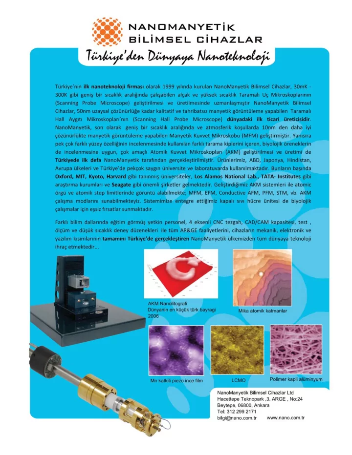
SPECS is specialized in the development and production of customized UHV surface analysis systems. Following the customer's vision, SPECS conceives, designs, and produces individual systems to meet the customer's needs. In our customized UHV surface analysis systems, sample preparation facilities like MBE , sputtering , and thin film deposition are combined with in-situ analysis by our ultra high resolution XPS analyzer PHOIBOS, by LEED diffraction and by imaging techniques like STM , LT- STM , and LEEM/PEEM . A large variety of excitation sources can be mounted on our UHV vacuum chambers. All systems are accompanied by a powerful and easy to handle software speeding up the acquisition and analysis of scientific data. Surface science provides deep insights into the properties of matter which are indispensable when developing new products and applications for tomorrow's world: nanotechnology, information technology, medicine, materials science, environmental protection, production of energy.The research tasks require surface analysis systems of the highest standards. SPECS meets these requirements by pooling and combining the company's expertise with that of Bestec, CreaTec and Surface Concept within the Network of Competence. unavailable. Electron Spectrometers Scanning Probe Microscopy Sources LEEM/PEEM LEED Thin Film Growth REPRESENTED IN TURKEY BY Hacettepe Teknokent Kuluçka Merkezi Arge Binası No : 31, 06800 Beytepe, Ankara TEL : +90 312 299 2171 FAKS : +90 312 299 2173 www.nano.com.tr --- bilgi@nano.com.tr
Oral Presentation, Theme E : Nanoelectronics, Spintronics, Nano-Magnetics, Quantum Computing, Qubits Monolayer-directed Assembly and Magnetic Properties of FePt Nanoparticles on Patterned Aluminum Oxide Oktay Yildirim, 1,2* Tian Gang, 3 Sachin Kinge, 3,4 David N. Reinhoudt, 1,4 Dave H.A. Blank, 2 Wilfred G. van der Wiel, 3 Guus Rijnders 2 and Jurriaan Huskens 1 1 Molecular Nanofabrication Group 2 Inorganic Materials Science 3 SRO NanoElectronics 4 Supramolecular Chemistry & Technology MESA+ Institute for Nanotechnology, University of Twente, P.O. Box 217, 7500 AE, Enschede, The Netherlands Abstract— Modification of Al 2 O 3 surfaces with self-assembled monolayers (SAMs) of phosph(on)ates with terminal functional groups resulted in FePt NPs assembly via ligand exchange. Patterning the substrates by microcontact printing allowed local nanoparticle assembly. Thermal annealing led to phase transformation of the NPs which resulted in ferromagnetic behavior at room temperature. By nanoimprint lithography FePtAu patterns at micron and nanoscale with high contrast between patterned and non-patterned regions were created. Electrical measurements showed that SAM formed an insulating barrier on conducting metal oxide. Recently, ferromagnetic nanoparticles have attracted great (Figure1). Thermal annealing under N 2 /H 2 reducing interest due to their high chemical stability, hard magnetic environment leads to a phase change of FePt from chemically properties and small size which makes them good candidates disordered FCC to chemically ordered FCT phase which to be used at spintronic devices, magnetic sensing and results in ferromagnetic behaviour at room temperature with ultrahigh density data storage applications [1]. Synthesis, around 440 Oe coercivity (Figure2). Microcontact printing characterization and assembly of monodisperse FePt ( μ CP) provides the possibility to direct the NP assembly to nanopaticles have been extensively studied. FePt designated areas of the substrate. Self-assembly combined high magnetocrystalline anisotropy (10 8 nanoparticles have with phosph(on)ate based PNDA, ABP, MUP self assembled erg/cm 3 ), which indicates, a 3nm particle has much higher monolayers (SAMs) having different end-groups is shown to magnetic anisotropy energy than the thermal energy[1]. They be an effective tool to fabricate FePtAu patterns with high have higher chemical stability than other hard magnetic contrast between patterned and non-patterned regions with a materials[1]. Their well defined boundaries and small size are high resolution below 200 nm as well as in micron range by using nanoimprint lithography (NIL). To use the (SAMs) in spintronic devices, to be able to fabricate electrical contacts 1,00E-007 1,00E-007 1,00E-007 1,00E-007 1,00E-007 1,00E-007 and to have information on electrical properties of SAM layers 5,00E-008 5,00E-008 5,00E-008 5,00E-008 5,00E-008 5,00E-008 is necessary. Electrical characterization of the SAMs on M ( A m ^2 ) M ( A m ^2 ) M ( A m ^2 ) M ( A m ^2 ) M ( A m ^2 ) M ( A m ^2 ) 0,00E+000 0,00E+000 0,00E+000 0,00E+000 0,00E+000 0,00E+000 conducting metal oxide Nb doped SrTiO 3 (NbSTO) by cyclic -6 -6 -6 -6 -6 -6 -4 -4 -4 -4 -4 -4 -2 -2 -2 -2 -2 -2 0 0 0 0 0 0 2 2 2 2 2 2 4 4 4 4 4 4 6 6 6 6 6 6 H(kOe) H(kOe) H(kOe) H(kOe) H(kOe) H(kOe) -5,00E-008 -5,00E-008 -5,00E-008 -5,00E-008 -5,00E-008 -5,00E-008 voltammetry (CV) showed the efficiency of SAM layer to M (A m2 ) M (A m2 ) M (A m2 ) M (A m2 ) M (A m2 ) M (A m2 ) 1 ,0 1 1 ,0 ,0 1 1 ,0 ,0 1 ,0 00 00 E- 0 0 E- 00 00 0 E- 00 E- 0 E- 00 0 0 E- 7 7 7 7 7 7 -1,00E-007 -1,00E-007 -1,00E-007 -1,00E-007 -1,00E-007 -1,00E-007 5 ,0 ,0 5 5 ,0 5 5 5 ,0 ,0 ,0 0 00 E- E- 0 0 E- 00 00 E- 0 00 E- 00 0 0 E- 00 8 8 8 8 8 8 isolate the substrate from environment. Pt top contacts ^ 2 ) ^ 2 ) ^ 2 ) ^ 2 ) ^ 2 ) ^ 2 ) 0 0E ,0 0E 0 ,0 0E ,0 0 0 0E ,0 0E ,0 0 0 ,0 0E 00 00 + + + 00 + 00 00 + + 00 0 ,0 -1 ,0 0 -1 ,0 ,0 -1 -1 ,0 0 0 -1 ,0 0 0 -1 5 0, - 0, 5 5 0, - - - 0, - 0, 5 - 0, 5 5 0, 0, 0, 0, 0, 0, 0 0 0 0 0 0 0 0 0 ,5 ,5 0 ,5 ,5 ,5 0 ,5 0 1 1 1 1 1 1 ,0 ,0 ,0 ,0 ,0 ,0 M ( A m M ( A m M ( A m M ( A m M ( A m M ( A m H (k O e ) H (k O e ) H (k O e ) H (k O e ) H (k O e ) H (k O e ) ,0 -5 -5 ,0 -5 -5 ,0 ,0 ,0 -5 ,0 -5 0 0 E-0 E-0 E-0 E-0 0 0 E-0 0 E-0 0 0 8 8 8 0 0 0 0 8 8 8 0 (b) (b) (a) (a) (a) (a) (a) (a) -1 ,0 ,0 -1 ,0 -1 -1 ,0 -1 ,0 ,0 -1 E-0 0 E-0 E-0 E-0 0 0 E-0 0 0 E-0 0 7 7 0 7 0 0 7 0 0 7 0 7 fabricated by pulsed laser deposition (PLD) are isolated from -1,50E-007 -1,50E-007 -1,50E-007 -1,50E-007 -1,50E-007 -1,50E-007 -1 ,5 ,5 -1 -1 -1 ,5 -1 ,5 ,5 ,5 -1 E-0 0 E-0 0 0 E-0 0 E-0 0 E-0 E-0 0 0 7 0 7 0 7 0 7 0 0 7 7 the susbtrate by SAM layer. When compared to bare NbSTO Figure 1: (a) AFM of FePt nanoparticles assembled on ABP/Al 2 O 3 surface. (b)VSM of FePt nanoparticles assembled substrate, organic layer on NbSTO has similar effect with an at 800 o C under H 2 /N 2 on PEI/Al 2 O 3 surface and annealed 4 nm Al 2 O 3 layer on NbSTO and causes a decrease in the environment . leakage current at same voltage range. The authors gratefully acknowledge support from the MESA+ Institute for very suitable to have storage densities in order of terabit/inch 2 Nanotechnology (SRO Nanofabrication) and NanoNed, the with reduced noise. Nanotechnology network in The Netherlands. This work is To be able to use FePt nanoparticles having high part of WGvdW’s research program ‘Organic materials for magnetocrystalline anisotropy for magnetic data storage spintronic devices’, financially supported by the Netherlands applications, it is necessary to have control on the assembly Organization for Scientific Research (NWO) and the process and cover a sizeable area with high packing density. Technology Foundation STW. We acknowledge Mark Although most of the study has been done on FePt NPs on Smithers for TEM and Gerard Kip for XPS measurements. We SiO 2 substrates, Al 2 O 3 is a better candidate to be used as thank A. Wagenaar and J. Engbersen (RUG, Groningen) for substrate instead of SiO 2 because Al 2 O 3 is an important providing TDP. dielectric material used in electronic device fabrication and the mostly used dielectric in magnetic tunneling junctions (MTJs) and a more electrically resistant material than SiO 2 . *Corresponding author: o.yildirim@tnw.utwente.nl Besides, Al 2 O 3 may be a model system for other FePt/metal oxide systems. [1] S. H. Sun, S. Anders, T. Thomson, J. E. E. Baglin, M. F. Toney, We demonstrate a method to assemble FePt nanoparticles on H. F. Hamann, C. B. Murray and B. D. Terris, Controlled Synthesis Al 2 O 3 surface in a controlled way via assembly and ligand and Assembly of FePt Nanoparticles , J. Phys. Chem.B, 2003, 107, exchange of FePt NPs on polyethyleneimine (PEI), 5419-5425. aminobutyl phosphonic acid (ABP) or phosphonoundecanoicacid (PNDA) modified Al 2 O 3 surfaces 109 6th Nanoscience and Nanotechnology Conference, �zmir, 2010
Recommend
More recommend
Explore More Topics
Stay informed with curated content and fresh updates.
