Device Layer-Aware Analytical Placement for Analog Circuits Biying - PowerPoint PPT Presentation
The picture can't be displayed. Device Layer-Aware Analytical Placement for Analog Circuits Biying Xu 1 , Shaolan Li 1 , Chak-Wa Pui 2 , Derong Liu 3 , Linxiao Shen 1 , Yibo Lin 1 , Nan Sun 1 , David Z. Pan 1 1 ECE Dept., the University of Texas
The picture can't be displayed. Device Layer-Aware Analytical Placement for Analog Circuits Biying Xu 1 , Shaolan Li 1 , Chak-Wa Pui 2 , Derong Liu 3 , Linxiao Shen 1 , Yibo Lin 1 , Nan Sun 1 , David Z. Pan 1 1 ECE Dept., the University of Texas at Austin 2 CSE Dept., the Chinese University of Hong Kong 3 Cadence Design Systems, Inc. 1
Outline Introduction of Device Layer-Aware Analog Placement Device Layer-Aware Analog Placement ü Non-linear optimization based global placement ü Linear programming based legalization and detailed placement Experimental Results Summary 2
Analog IC Trend High demand in emerging applications: Internet of Things (IOT), autonomous and electric vehicles, communication and 5G networks Communication Sources: IBM Advanced computing Healthcare 3
Analog Layout Automation Challenges Modern SoCs: 20% or less analog, but maybe over 80% design time Analog IC layout design still heavily manual ü Cf. digital IC layout automation ü Very time-consuming, tedious, and error-prone Some prior work on analog placement ü [Lampaert+, JSSC’95], [Strasser+, ICCAD’08], [Ma+, TCAD’11], [Wu+, ICCAD’12], [Lin+, TCAD’16], [Ou+, TCAD’16] Limitations of previous approaches ü Efficiency and scalability issues for stochastic or enumerative approaches ü Still limited to consider complex scenarios and characteristics unique to analog designs, which can contribute to better layout quality 4
Introduction Analog circuits often contain different types of devices Sometimes overlaps are allowed and beneficial Circuit example: capacitive-coupled OTA ü 30% and 4% area and wirelength reductions, respectively VDD VBP C C C C Bias and CMFB not shown C F C F V OP V ON C s C s CMFB VBN VBN VBN V IP V IN Phase Margin Unity Gain Loop Gain Layout (deg.) Bandwidth (MHz) (dB) Non-overlap 71.9 103.7 36.3 overlap 71.5 105.4 36.3 5 30% area reduction
Introduction Circuit example: current-controlled Center Frequency Tuning Gain Layout ring oscillator (CCO) (f CCO ) (kHz) (k CCO ) (THz/A) Non-overlap 609 0.89 ü 30% and 20% area and wirelength overlap 610 0.90 reductions, respectively I CTRL I CTRL I O I O C L C L CCO Delay Cell 6 30% area reduction
Our Contributions Consider device-specific overlapping in analog circuits during placement, which offers high flexibility for layout optimization ü Devices that are insensitive to coupling and built on mutually exclusive layers are allowed to overlap A holistic analytical framework to solve the device layer-aware analog placement problem An analog global router is developed to verify the routability of our device layer-aware placement results 7
Preliminary Type I devices can overlap Type II devices without degrading circuit performance Device types are specified by circuit designers Type I devices: built without metal or via layers, and not sensitive to coupling, e.g. some Vb transistors and resistors Vin+ Vin- M 1 M 2 M 7 M 8 Type II devices: built only with metal and via layers, and not sensitive to coupling, e.g. some metal-oxide-metal capacitors V o- Vcmi Vo+ Type III devices: occupying not only the metal and via layers but also substrate and polysilicon layers, M 5 M 6 M 3 M 4 or the device that is critical and sensitive to Vcmfb coupling, e.g. some pre-laid-out sub-circuits or sensitive devices An analog circuit example 8
Device Layer-Aware Analog Placement Inputs: Device Layout Placement Circuit Types & Constraints Boundary Netlist Shapes ü Circuit netlist ü Device sizes and designer specified device types Device Layer-Aware Analog Placement Global Placement ü Analog layout constraints (e.g., symmetry) CG-based Non-linear Optimization ü Placement boundary (as generated from desired Adjust Coefficients in Objective utilization rate and aspect ratio) Legalization Output: a legal placement solution Constraint Graph Construction Objectives: Symmetry-Aware Legalization ü Total area Detailed Placement ü Total wirelength Placement Result Overall flow 9
Device Layer-Aware Analog Placement Constraints: ü Symmetric device group shares a common symmetric axis in the placement 1 7 3 6 4 2 8 5 10 9 a symmetric group with vertical symmetric axis An analog placement example ü Device-specific overlapping constraints: o Devices built by mutually exclusive manufacturing layers and insensitive to coupling are allowed to overlap each other; while others are not ü Placement boundary constraint 10
Global Placement We relax the constraints into penalties in the objective, and transform the problem into an unconstrained nonlinear optimization problem Objective: 8 7 !"#$%&'($ = * +, + . / * 0, + " / * 123 + % / * + * 456 456 Wirelength term (half-perimeter wirelength): * +, = Σ : ; (max @∈: ; B @ − min @∈: ; B @ + max @∈: ; F @ − min @∈: ; F @ ) Device-specific overlap penalty: x = x A+ w A- x B 7 / ! @,J O A,B 8 * 0, = H ! @,J @,J ∈, A 7 = max min B @ + K @ − B J , B J + K B ! @,J J − B @ , K @ , K J ), 0 y = h B O A,B 8 = max min F @ + ℎ @ − F J , F J + ℎ J − F @ , ℎ @ , ℎ J ), 0 ! @,J 11
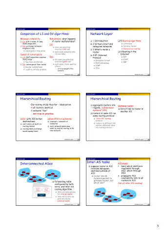
Global Placement Asymmetry penalty: 6 7 + 7 + ' % 6 7 ! = ' ' 0 , + 0 . − 2 4 0 5 8 , − 8 . 0 , − 0 5 "#$ / 9 ( ) ∈+ ,∈( ) ,,. ∈( ) A B C (x A ,y A ) (x B ,y B ) (x C ,y C ) c Out of boundary penalty: xk ! :;< = ' max 0 @ − 0 , , 0 + max 0 , + B , − 0 C , 0 + max 8 @ − 8 , , 0 + max 8 , + ℎ , − 8 C , 0 ,∈< i x i 12 x L x H
Global Placement Log-sum-exp (LSE) to smooth max and min functions 3 4 5 3 4 5 2 1 9 2 Smoothed max + * : - log 0 1 Smoothed min + * : −- log 0 * * * * The unconstrained nonlinear optimization problem is solved with nonlinear conjugate gradient method provided by WNLIB Iteratively update the weights of different terms in the objectives ü The weight of the wirelength term is larger than other weights at the beginning ü Weights of other terms are increased gradually, until the penalties are below certain thresholds ü The algorithm stops when all the penalties are below the preset thresholds, or after it reaches the preset max. #iterations WNLIB: W. Naylor and B. Chapman, http://www.willnaylor.com/wnlib.html 13
Legalization Constraint graph construction D D ü Plane sweep algorithm E E s [Doenhardt+, TCAD’87] h B B A ü Solid edges: horizontal; dashed A edges: vertical C C s v D Device layer-aware constraint B E D graph construction A E s h A B C C Type I Type II Type III s v 14
Legalization D D E s E h B B D A E B A A C C C s v (a) Global placement result (c) Constraints graphs after greedily example w/ illegal device overlaps determining overlap edges D D E E s s h h B B D D A A E B B C C E A A C C s s v v (b) Constraint graphs after applying (d) Constraints graphs after missing plane sweep algorithm positional relationship detection 15
Legalization Linear programming (LP)-based legalization to minimize area Decomposed into x- and y- direction sub-problems and solved independently Minimize ' Subject to 0 ≤ 1 2 ≤ ' − 4 2 , ∀7 ∈ 9, Boundary constraints 1 2 + 4 2 ≤ 1 ; , ∀< 2,; ∈ = > , Topology order constraints F , C , ∀ 7, D ∈ E B 1 2 + 1 ; + 4 ; = 2 A 1 B ∀E B ∈ =, Symmetry constraints C , ∀7 ∈ E B G , 2 A 1 2 + 4 2 = 2 A 1 B Minimize H Subject to 0 ≤ I 2 ≤ H − ℎ 2 , ∀7 ∈ 9, Boundary constraints I 2 + ℎ 2 ≤ I ; , ∀< 2,; ∈ = K , Topology order constraints F , ∀E B ∈ =, I 2 = I ; , ∀ 7, D ∈ E B Symmetry constraints 16
Detailed Placement LP-based wirelength refinement Minimize '()*+*,-.ℎ 0 ≤ 9 : ≤ ' ∗ − = : , ∀( ∈ A, Subject to Fixed boundary and 9 : + = : ≤ 9 C , ∀* :,C ∈ D E , topology order 0 ≤ F : ≤ G ∗ − ℎ : , ∀( ∈ A, constraints F : + ℎ : ≤ F C , ∀* :,C ∈ D H , O , M , ∀ (, N ∈ - L 9 : + 9 C + = C = 2 K 9 L M , ∀( ∈ - L P , ∀- L ∈ D, 2 K 9 : + = : = 2 K 9 L Symmetry constraints O , F : = F C , ∀ (, N ∈ - L 17
Experimental Results All algorithms are implemented in C/C++ All experiments are performed on a Linux machine with 3.4GHz Intel(R) core and 32GB memory. Benchmark information Design # Devices # Type I # Type II # Type III # Nets Devices Devices Devices opamp 46 42 4 0 29 g m -C 15 13 2 0 9 integrator 21 6 2 13 27 CTDSM 18
Experimental Results Compare effects of device layer awareness NLP Without Device Layer Awareness Device Layer-Aware NLP Design Area (µm 2 ) HPWL (µm) Run-time (s) Area (µm 2 ) HPWL (µm) Run-time (s) Actual Norm. Actual Norm. Actual Norm. Actual Norm. Actual Norm. Actual Norm. opamp 2972.7 1 753.2 1 17.1 1 2369.9 0.797 497.7 0.661 10.9 0.637 g m -C 182.0 1 72.8 1 1.2 1 175.1 0.962 60.5 0.831 1.2 1.000 integrator CTDSM 57454.5 1 3129.4 1 6.5 1 56059.8 0.976 2580.0 0.824 6.5 0.997 Average 1 1 1 0.912 0.772 0.878 19
Experimental Results 9% and 23% area and HPWL reductions, respectively, when considering device-specific overlapping 1 . 2 1 . 2 NLP NLP Device Layer-Aware NLP Device Layer-Aware NLP 1 . 0 1 . 0 Normalized HPWL Normalized Area 0 . 8 0 . 8 0 . 6 0 . 6 0 . 4 0 . 4 0 . 2 0 . 2 0 . 0 0 . 0 g m -C integrator g m -C integrator opamp CTDSM opamp CTDSM Circuit Benchmarks Circuit Benchmarks 20
Recommend
More recommend
Explore More Topics
Stay informed with curated content and fresh updates.

