Defects in Crystalline Solids: the Basics Arkady Krasheninnikov - PowerPoint PPT Presentation
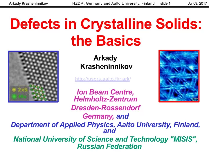
Arkady Krasheninnikov HZDR, Germany and Aalto University, Finland slide 1 Jul 09, 2017 Defects in Crystalline Solids: the Basics Arkady Krasheninnikov http://users.aalto.fi/~ark/ Ion Beam Centre, Helmholtz-Zentrum Dresden-Rossendorf
Arkady Krasheninnikov HZDR, Germany and Aalto University, Finland slide 1 Jul 09, 2017 Defects in Crystalline Solids: the Basics Arkady Krasheninnikov http://users.aalto.fi/~ark/ Ion Beam Centre, Helmholtz-Zentrum Dresden-Rossendorf Germany, and Department of Applied Physics, Aalto University, Finland, and National University of Science and Technology "MISIS", Russian Federation
Arkady Krasheninnikov HZDR, Germany and Aalto University, Finland slide 2 Jul 09, 2017 Outline of the tutorial lecture 1. Introduction: Why do we care about defects in crystalline solids? 2. What we already know: defects in bulk systems, their classification and origin. 3. Basic formula for defect concentration at thermodynamic equilibrium; 4. Overview of experimental techniques for Courtesy of J. M eyer defect identification 5. Overview of frequently used atomistic appro- aches to get insights into defect behavior 6. Defects in two-dimensional materials: Why interesting? Courtesy of K. Suenaga
Arkady Krasheninnikov HZDR, Germany and Aalto University, Finland slide 3 Jul 09, 2017 Some basics of defects in solids: Repetitio est mater studiorum
Arkady Krasheninnikov HZDR, Germany and Aalto University, Finland slide 4 Jul 09, 2017 Defects in crystalline solids Ø What are defects? In general, structural imperfection in a crystal, vacancy deviation from the perfect order (periodicity) Note that defects can also be defined in amorphous systems and quasicrystals — interstitial beyond the scope of the lecture Ø Why do we care about defect? They frequently govern materials properties: • Mechanical (e.g. dislocations in metals) • Electronic (e.g. dopant atoms in semiconductors) • Optical (e.g., color centers in wide-gap semiconductors) • Magnetic (impurity atoms; coordination defect) • Also responsible for diffusion of atoms in the solid, etc. Ashcroft-Mermin: “Like human defects, those of crystals come in a seemingly end- less variety, many dreary and depressing, and a few fascinating.”
Arkady Krasheninnikov HZDR, Germany and Aalto University, Finland slide 5 Jul 09, 2017 Defect (more thorough) definition A structural defect is a configuration in which an atom (or group of atoms) does not satisfy the structure rules pertaining to the ideal reference system or material. Are defects in solids really the “bad” guys? - + Deterioration of mechanical Improvement of mechanical Ø Ø properties properties in some systems Break down of electronic Doping Ø Ø devices Providing bright colors Ø Non-radiative transitions Ø Pinning of magnetic vortices in Ø Undesirable magnetism type II superconductors Ø
Arkady Krasheninnikov HZDR, Germany and Aalto University, Finland slide 6 Jul 09, 2017 Example of when the defects strengthen the material Mechanical properties of carbon nanotube paper Experiment: J. J. Åström et al. , PRL 93 (2004) 215503. ~ 15 nm ~ 4 µ m ~ 1 cm Simulations: ~ 1 nm The continuum theory model with parameters derived ~ 50 µ m from atomistic simulations
Arkady Krasheninnikov HZDR, Germany and Aalto University, Finland slide 7 Jul 09, 2017 Classification of defects in crystalline solids Ø How can we classify them? According to their dimensionality: vacancy • Point defects (e.g. vacancies) 0D defects • Linear defects (e.g. dislocations) 1D defects • Planar defects (grain boundaries) 2D defects interstitial • Volume defects (voids) 3D defects Disclination (in 2D) dislocation Note that in 2D systems 2D and 3D defects do not exist According to their origin: • Native (pre-existing in the sample) • Irradiation- (or, e.g., chemical-treatment)-induced
Arkady Krasheninnikov HZDR, Germany and Aalto University, Finland slide 8 Jul 09, 2017 Classification of defects in crystalline solids Ø How can we classify them? According to their thermodynamics (concentration): • In thermodynamic equilibrium (relevant to point defects only) • Non-equilibrium (e.g. irradiation-induced defects) According to sample chemical content (elemental solids, compounds): • Intrinsic (e.g., vacancies, interstitials) • Extrinsic (impurity atoms) • Antisites (in compound solids) • Chemically equivalent: isotopes (vibrational properties) According to the local number of atoms: • Missing/extra atoms (e.g., vacancies, interstitials) 7 • Wigner defects, e.g., Stone-Wales 5 5 defects in graphene, rotational defects in TMDs, metastable I-V complexes in Si 7 or graphite • Topological defect
Arkady Krasheninnikov HZDR, Germany and Aalto University, Finland slide 9 Jul 09, 2017 Energetics of point defects in monatomic solids Ø Schottky defect to infinity formation energy: to an empty site at the E f = E(N-1) + E(1) – E(N) surface E f = E(N-1) + E(N)/N – E(N) E f > 0 !!! N is the number of atoms in the system Ø Frenkel defect formation energy: E f = E(N with iv pair) – E(N) E f = E f (vac) + E f (inter) E f > 0 !!!
Arkady Krasheninnikov HZDR, Germany and Aalto University, Finland slide 10 Jul 09, 2017 Formation energies of some point defects Ø In general, let’s define formation energy of an electrically neutral point defect (vacancy/interstitial) as : E f = E tot ( with defect ) – E tot ( without defect ) ± µ where µ is chemical potential of the missing/extra atom Ø For substitutional impurities (e.g., N atom in graphene): E f = E tot ( with defect ) + µ C – E tot (without defect ) –µ N Ø For defects in compounds (e.g. C impurity in BN) another condition should be met: E f = E tot ( with defect ) + µ N – E tot ( without defect ) –µ C E f = E tot ( with defect ) + µ BN – µ B – E tot ( without defect ) –µ C So called, N-rich and B-rich conditions; In general, E f is a function of chemical potentials (choose ones matching the experimental situation)
Arkady Krasheninnikov HZDR, Germany and Aalto University, Finland slide 11 Jul 09, 2017 Where do defects come from? Ø Defect formation energy is positive: it costs energy to create a defect; Why do we have then defects in solids at finite temperatures ? Ø Assume: vacancy concentration is low (defects do not interact) T = const P = const The Gibbs free energy of the crystal: Ø G = G 0 + nE f – TS , where G 0 = Gibbs energy of the ideal crystal; n = N v / N n = defect concentration; E f > 0 = energy required to create a vacancy N ! S = configurational entropy S = k B ln ( N − N v )! N v !
Arkady Krasheninnikov HZDR, Germany and Aalto University, Finland slide 12 Jul 09, 2017 Where do defects come from? The Gibbs free energy of the crystal: ~ E f n ~ hn G = G 0 + nE f – TS At thermodynamic equilibrium: energy ¶ G / ¶ n = 0 G = E f n - TS G = hn - TS E f - T ¶ S / ¶ n = 0 n = N v / N; N v << N ~ - TS N ! ln x! » x lnx -x, x à ¥ S = k B ln n,defect concentration ( N − N v )! N v ! equilibrium ( ) n = N v / N L = exp − E f / k B T concentration Ø Entropy gives rise to appearance of point defects at finite temperatures Ø Synthetic materials (or e.g., subjected to irradiation) concentration of defects may be different from equilibrium
Arkady Krasheninnikov HZDR, Germany and Aalto University, Finland slide 13 Jul 09, 2017 Typical defect formation energies in bulk solids Al: melting Tm = 933K T = 300K, n = 3 10 -12 T = 800K, n = 2 10 -4 exp(2.4) » 10 (prefactor) Small exercise SW defect in graphene, E f = 4-5 eV ( ) How many = = - D + D n N / N exp h / k T s / k v L f B f B defects at 300K?
Arkady Krasheninnikov HZDR, Germany and Aalto University, Finland slide 14 Jul 09, 2017 Experimental methods used to detect and characterize defects in materials (also elemental analysis techniques to detect impurities) Ac Accelerator sputtered Ac Accele- sample ra rator atoms
Arkady Krasheninnikov HZDR, Germany and Aalto University, Finland slide 15 Jul 09, 2017 Methods of defect characterization (an overview) Indirect methods: concentration finite defect Optical spectroscopy Main idea: detection of optical transitions associated with defects required Electron paramagnetic resonance Main idea: detection of localized electron magnetic moments Raman spectroscopy Main idea: detection of new phonon modes associated with defects X-ray absorption spectroscopy and related methods (XAFS,XANES) Main idea: probing the electronic states associated with defects by exciting core electrons Positron annihilation spectroscopy (does not work for 2D materials) Main idea: a positron gets stuck on the vacancy;we detect the photons which appear upon its annihilation with an electron Detection of Direct methods: defects is individual Scanning probe microscopy possible Main idea: getting an image of a particular defect on the surface Transmission electron microscopy Main idea: getting an image of a particular defect in a thin slice
Arkady Krasheninnikov HZDR, Germany and Aalto University, Finland slide 16 Jul 09, 2017 Electron spin (paramagnetic) resonance (ESR/EPR) Assume we have Example: dangling bond at unpaired localized atoms near vacancies in electrons semiconductors The main idea: We can detect the magnetic moment associated with the spin of the unpaired electron Let’s apply a steady magnetic field B 0 E 0 = + µ E E m g B 0 s e B 0 = ± » (the Lande Factor m 1 / 2 ; g 2 ) s e µ = e ! / 2 m (the Bohr magneton ) B e
Recommend
More recommend
Explore More Topics
Stay informed with curated content and fresh updates.
