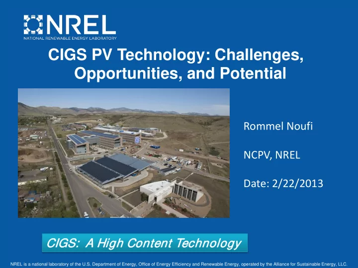
CIGS PV Technology: Challenges, Opportunities, and Potential Rommel - PowerPoint PPT Presentation
CIGS PV Technology: Challenges, Opportunities, and Potential Rommel Noufi NCPV, NREL Date: 2/22/2013 CIGS: A H High C gh Cont ontent nt T Technol hnology ogy NREL is a national laboratory of the U.S. Department of Energy, Office of
CIGS PV Technology: Challenges, Opportunities, and Potential Rommel Noufi NCPV, NREL Date: 2/22/2013 CIGS: A H High C gh Cont ontent nt T Technol hnology ogy NREL is a national laboratory of the U.S. Department of Energy, Office of Energy Efficiency and Renewable Energy, operated by the Alliance for Sustainable Energy, LLC.
Outline • Review: State of the CIGS technology • Technical Challenges • Opportunities: Efficiency and Cost • Potential: - Closing the gap between laboratory cells & modules - Cost ? $ 0.50 module + 0.50 BOS = $1/W Acknowledgement: Thin Film Group, M&C Group, and Alan Goodrich Rommel.noufi@nrel.gov Innovation for Our Energy Future 2
CIGS Device Structure ZnO, ITO 2500 Å CdS or ZnS 500 Å CIGS 1-2.5 µm Mo 0.5-1 µm Glass, Metal Foil, Plastics Innovation for Our Energy Future 3
Parameters of High Efficiency CIGS Solar Cells J sc (mA/cm 2 ) Sample Number V oc (V) Fill factor (%) Efficiency (%) ZSW 0.740 35.40 77.5 20.3 ZSW M2992-11 0.690 35.55 81.2 20.0 NREL S2229A1-3 0.720 32.86 80.27 19.0 S2229A1-5 0.724 32.68 80.37 19.0 S2229B1-2 0.731 31.84 80.33 18.7 C3010-22-4 0.803 29.15 79.47 18.6 AIST, Monolith Flex. Module 11.60 (0.683) 34.00 68.40 16.0 (75 cm 2 ) EMPA, Polyimide 0.670 34.00 74.10 16.9 (18.6) NREL, Nakada , SS 0.650 36.38 74.20 >17.5 Tolerance to wide range of molecularity Cu/(In+Ga) 0.95 to 0.82 Ga/(In+Ga) 0.26 to 0.55 Yields device efficiency of 18% to >20% Innovation for Our Energy Future 4
“High End” Modules from MFG Line (pilot line) Company Device Aperture Area (cm 2 ) Efficiency (%) 0.985 m 2 Stion CIGS (glass) 14.5 AVANCIS CIGSS (glass) 4938 (26 x 26) 13.0 (15.5) Solar Frontier CIGSS (glass) 3600 (30 x 30) 13.0 (18) 0.684 m 2 (cell) Solibro CIGS (glass) 14.4 (17.4) 8390 (120 cm 2 ) Global Solar CIGS (flexible) 13.0 (15.3) 1.2 m 2 (cell) Miasole CIGS (flexible) 15.7 (17.5) 0.33 m 2 (120 cm 2 ) Solopower CIGS (flexible) 13.5 (15.1) 30 x 30 cm 2 TSMC CIGSS (glass) 15.7 (16.4) First Solar CdTe (glass) 6623, high volume 12.7 (16 champ) Innovation for Our Energy Future 5
Technical Challenges Large impact on performance and cost Innovation for Our Energy Future 6
Targeted Metrics for the roadmap (Efficiency improvements and cost reductions) Metrics Current State of Art Proposed Targets Cost Reduction Laboratory Commercial Laboratory Commercial (W PDC ) Enhance efficiency (%) 20.00 12.00 22.00 >16.00 V OC (volts) 0.70 0.60 0.75 0.70 $0.12 J SC (mA/cm 2 ) 35.40 30.00 36.50 34.00 $0.07 FF 0.80 0.66 0.80 0.70 $0.04 Subtotal (efficiency-related reductions) $0.23 0.15 0.50 Rapid CIGS growth $0.12 µm/min µm/min 70-nm 70-nm 20-nm CdS; 20-nm CdS; $0.05 Alternative buffer wet CdS wet CdS 70-nm 70-nm sputtered & ZnS sputtered ZnS ZnS Subtotal (area-related cost reductions) $0.17 Total (area- and efficiency-related cost benefits) $0.40 V OC = open-circuit voltage; J SC = short-circuit current density; FF = fill factor; W PDC = Watt peak direct current Innovation for Our Energy Future 7
Higher efficiency through higher photovoltage Goal: Demonstrate V oc between 0.75 and 1.0 V for Ga content between 30 and 100% with efficiencies higher than the state of the art. Relevance: Being able to maintain high efficiency (>20% as in low Ga cells) while raising the Ga content of the cell relative to In content, allows progress toward higher theoretical efficiency. The cost reduction opportunity is about $0.12/W Innovation for Our Energy Future 8
Efficiency / V OC vs Band-gap / Composition The Challenge: High Efficiency Across the Whole Composition Range Current baseline Previous baseline Theoretical limit Efficiency (%) Absorber band gap (eV) Innovation for Our Energy Future
Voc is limited to a certain value Innovation for Our Energy Future
Results: EBIC/EQE Eg~1.1 eV Eg~1.2 eV Eg~1.4 eV • as the Ga content is increased, the overall collection of the cells decreases predominantly for the longer wavelengths (diff. length) • highest bandgap materials, such as the CuGaSe 2 case, also show an overall lower collection efficiency (<90%) in the visible wavelengths, an indication additional recombination is further limiting the performance of such cells (interface recombination?) Eg~1.6 eV Key findings: (a) loss of collection efficiency as Ga is increased (b) Existence of random and discrete electronically inactive grains in carrier generation/collection ANALYTICAL MICROSCOPY GROUP: origin of inactive grains and/or interfaces (chemical, structural, optoelectronic studies of grains and grain boundary ) Innovation for Our Energy Future 11
E le c tr onic Pr ope r tie s of Gr ain Boundar ie s in the Ce lls Impr ove d High- Ga CIGS Solar Innovation for Our Energy Future
Grain/Grain Boundary Structure Model Cu-depleted/ inverted layer/ e - -rich Hole barrier e – h + Space e – h + charge p-Type core/ hole-rich Neutral region Mo Cu-poor Defect Layer • A surface region (of finite thickness) including GBs exists which is Cu-deficient relative to the bulk of the grains • Cu-vacancies result in decrease in p-d repulsion. The latter causes a lowering of the E V maximum, and effectively an increase in E g – See: Albin et al, MRS Proc. , 228, p. 267, 1992; Jaffe et al, Phys. Rev. B27, 5167 (1983); B29, 1882, (1984) – As a result, a barrier is created that repels holes from the surface and GBs. 03562808-2 Innovation for Our Energy Future
Possible physical origin—electronic issue trap level CIS CGS Innovation for Our Energy Future
Previous defect calculations in CIS/CGS S. B. Zhang et al, 1998 Innovation for Our Energy Future
CIS CGS a) Cu vacancies are the main source of hole carrier density b) Antistie defects like neutral Cu In and In Cu are the most important deep traps in CIS/CGS. c) Mcu +2 is the most important deep traps that influences the Voc of CIGS. d) Vse is not important. Innovation for Our Energy Future
M Cu + 2V Cu : benefit the CIGS with Ga<50% Innovation for Our Energy Future
How to reduce the M Cu density? Innovation for Our Energy Future
How to reduce the M Cu density? a) Introducing Cu 2-x Se during the growth process, which is naturally Cu poor. More M Cu will be combined with V Cu to form complexes . In, Ga, Se Cu 2-x Se In, Ga, Se Innovation for Our Energy Future
How to reduce the M Cu density? b) Lower the growth temperature (e.g., grow at 450 K, work at 300 K) CIS CGS 1) The defect density of M Cu is large reduced in a large range of Cu chemical potential. 2) More growth time is needed to reach thermal equilibrium. Innovation for Our Energy Future
Potential Benefits of High Eg CIGS • High efficiency across the whole Ga range, Eg (1.1 to 1.7 eV) – easier composition control. • A wide range of Voltage/Current combination modules. • High band gap/high V oc reduces Power Temperature co-efficient. • Reduction of In by a factor of 2-3X. • Open the door for a high efficiency top cell for two-junction cells. Innovation for Our Energy Future 21
Higher cell efficiency through higher photocurrent and lower cost through streamlined process Goal: Demonstrate a >20% efficient CIGS device, using ZnO x S 1-x Relevance: The buffer/emitter layer in the CIGS device has been identified as high impact barrier for both efficiency and area related cost reduction. Deposition methods : CBD, ALD, Sputter The estimated cost reduction opportunity is about $0.13/W. Innovation for Our Energy Future 22
Higher Cell Efficiency through Higher Photo Current 1. The best J sc value obtained in the record CIGS solar cells is still quite lower than that achieved in Si (similar bandgap) 2. Great gains in efficiency could be attained if increased photocurrents are attained by maintaining V oc and FF values 3. The window materials (TCOs and CdS) are responsible for the absorption of photns that otherwise could generate Be Best st ca case se sce scenario: additional photocurrent Potential for efficiency = 20. 20.3% % x ( (40. 40.5/35. 35.4) = ) = 23. 23.2% Innovation for Our Energy Future 23
Design of Junction Interface with ZnOS layers Optical Bowing in ZnOS system Amorphous From published reports, we understand that: two-phase region Targeted range • Pure ZnS layer blocks the photocurrent (> 1 eV conduction band spike). • Pure ZnO layer presents a cliff and increased interface recombination. Data from sputtering, substrate temperature 200C • Optimum band gap and band offset (efficiency) can be obtained by Grimm, et. al., Thin Solid Films 520 (2011) 1330 careful choice of the alloy composition. Innovation for Our Energy Future
Transmission of ZnOS films Innovation for Our Energy Future
Recommend
More recommend
Explore More Topics
Stay informed with curated content and fresh updates.
